Hi, i'd like to ask for help in verifying a circuit i've designed (FPGA's core power supply). The constraints can be seen in the Excel spreadsheet (see images).
1) I used 1% tolerances for both the ballast resistors and the voltage regulation resistors. Is this ok, or is it worth looking for 0.1% components? (actually i did some tests with the spreadsheet and it doesn't seem to make much difference, but I'd like your opinion).
2) The optimal ballast resistor recommended by the Excel spreadsheet seems rather large and will produce a voltage drop. Will it be necessary to compensate for the LDO voltage, right? For example by adjusting output to 1.05V?
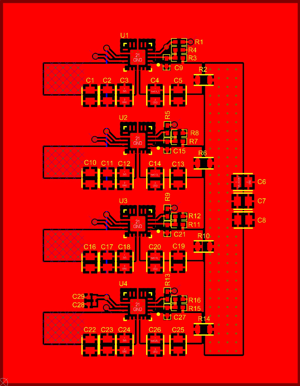
3) Is the physical layout ok? For the LDO output section, i've decided to avoid using traces, that could vary in resistance with temperature, and to use only the ballast resistors for the connection. what do you think?
Thank you, greetings