LM5137F-Q1: Output imbalance in single-output interleaved operation mode

Part Number: LM5137F-Q1
Other Parts Discussed in Thread: LM5137

I am using the LM5137F-Q1 with:

  • 24-42V input
  • 12V output (set via feedback resistors)
  • DRSS 10%
  • FPWM enabled
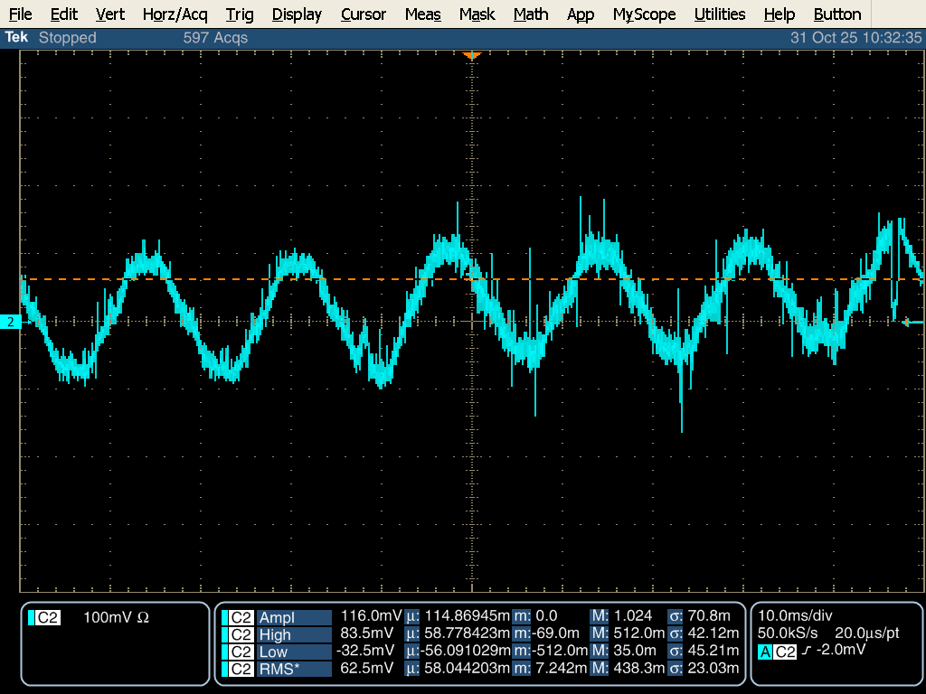
  • 0.5ohm load resistor (~24A total load current)

I'm seeing ~20% higher current being sourced from the secondary channel, where I would expect equal loading to primary and secondary.

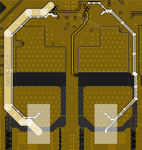
What could be possible causes to look for? Is this purely layout related?

  • Hello,

    Please send the schematic and a completed quickstart calculator. Reference the LM5137 EVM layout for a 2-phase design. Make sure to use wide aspect ratio shunt with low parasitic inductance.

    Regards,

    Tim

  • Here's a version showing DNP components...8741.Heater.pdf

  • Our secondary sync FET and inductor are consistently the highest temperature devices in the circuit, regardless of relation to the input or load, ie. there is a slight difference in trace length from the outputs to the load, and since there are multiple instances of this circuit with different placement relative to the load connection, we can compare the circuit performance to understand if the different in trace length to the load is a cause. It doesn't seem to be. I hope this drawing this helps to explain what I mean... The secondary is on the right. The next circuit alternates, with the primary being a shorter connection to the load.

    Still struggling to understand why there is an imbalance. An additional not is that with some extra heatsink cooling, we are seeing the imbalance drop a bit, secondary is 30% higher than primary without a heatsink, and secondary is 25% higher than primary with a heatsink.

  • Hi Stephen,

    There should be very little imbalance between the phases. Note we recommend using wide aspect ratio shunts to mitigate effects of parasitic inductance (although this should be similar for both phases). What you have here looks huge (long component => high inductance). Take a look at the 12V, 20A, 400kHz, 2-phase EVM for reference.

    Regards,

    Tim

  • The Y14840R00400F9R is described as non-inductive.

    Is the imbalanced trace length in the output connection to the load a problem? I see the EVM is very balanced, with the 2 outputs exactly mirrored. I didn't see this specific layout guidance mentioned.

  • Yes, the power stages should be well match ideally. However, if COMP1 and COMP2 are the same, both phases should get the same current command.

    I would check the CS voltage and see if there's an imbalance at the pins of the IC, as the shunts look very nonideal here (huge 3920 package, 5W rating seems like overkill, and the longer the package...the higher the parasitic inductance). Check the voltage at the CS pins.

    Regards,

    Tim

  • I have measured ~21.3mV on ISNS1+/BIAS1VOUT1 and ~26.3mV on ISNS2+/VOUT2. What changes should I make to make these equal? So far you've mentioned the change to a short body shunt, what about ISNS traces? The ISNS traces are on internal layers, but not on the immediately adjacent layer. Could that extra inductance be the culprit? I tried to replicate how those traces were placed in the EVM. The EVM has the shunt on the top layer, and the ISNS/VOUT traces on layer 5, I have shunt on bottom layer and ISNS/VOUT traces on layer 2.

  • Hi Stephen,

    Are those SW copper areas with vias? If so, that's likely the issue....noise coupled on to the CS lines. Check the differential voltage waveforms at the CS pins.

    Regards,

    Tim

  • Is this the noise you are referring to? It is definitely noisier than the EVM, which is shown in the second capture.

  • Do you recommend removing or keeping the CS signals well away from the SW copper areas? I need to keep the SW thermal pad and vias to couple to the heatsink on the opposite side of the PCB.

    FWIW, the bottom copper areas between the inductor and shunt will likely be removed, which are likely the closest coupling signals into the CS traces. These were added to try to help to get inductor heat out to the heatsink, but they don't seem to be doing much as the inductor is really only coupling heat out via the pads.

    Can you please share what the max expected current imbalance there should be? I couldn't find this specified in the electrical specs.

    Also, is there any tuning of the filter cap that could help to clean this signal up? 

  • Yes, keeping the CS traces away from SW is imperative. Also, SW shouldn't be used for heatsinking. Better to use VIN (drain of the high-side FET) for that. Refer to the EVM layout.

    Max current imbalance should be 10%.