UCC5304: Uncorrect Vgs signal of the Driver of high-side switch

Part Number: UCC5304


Hi everyone,

I'm currently trying to build a totem-pole PFC circuit, but I've found that my fast-leg drive circuit is generating an abnormal Vgs signal from the high-side switch during the positive half-cycle. (The high-side switch is regarded as a demagnetizing switch.)

1. Is there a design flaw? (The driver circuit is designed according to the datasheet.)

2. Or do I need to replace the driver to resolve this issue?


(Yellow : DSP signal of high-side switch /

 Green : Vgs signal of high-side switch /

 Blue : AC voltage /

 Pink : IL current )

messageImage_1763014014595.jpg


Best regards,

Eric Tsai

  • Hi Eric,

    Would you be able to provide a schematic? I would like to double check it just to be thorough.

    These abnormal short high pulses appear to be occurring before the input signal goes high. This leads me to believe that the low side FET switching is causing the VGS voltage change on the high side FET. I think double checking the schematic will help to narrow it down a bit further.

    Best regards,

    Will

  • Hi Will,

    Thank you for your reply.

    1.

    The following image is the circuit of my totem-pole PFC design, for your reference.

    (a. bridge rectifier, boost inductor, bulk capacitors & filter capacitors)

    (b. mosfet driver - "UCC5304", isolated power supply)

    (c. mosfet)


    2. 

    I found some information yesterday, but I'm currently unsure if the driver issue is caused by a hard switching problem in the circuit.

    I searched for relevant hardware solutions in this direction yesterday and found the TI - UCC5310M.

    I wonder if this would be a suitable solution for my current situation?

    Best regards,

    Eric Tsai

  • Hi Eric,

    Your schematic looks good. I do agree the issue appears to be related to hard switching. I would recommend to check out both the UCC5310MC and the UCC5350MC depending on the drive current spec you need. In addition, our team recently published an Application Brief that describes what a Miller Clamp pin feature can provide for your system, and I would recommend to check it out if you are curious to learn more. You can find it at the link below.

    https://www.ti.com/lit/ab/slya091/slya091.pdf

    Best regards,

    Will

  • Hi Will,

    1. I tested the driver circuit for the UCC5310MC today, but the problem persists.

    2. In your opinion, where could the problem be stemming from?

        Is this problem truly related to CGD?

    Best regards,

    Eric Tsai

  • Hi Eric,

    I have a few questions, if you are able to provide more information on these:

    1. Would you be able to provide a waveform of the switch node? I want to check if there is a transient on it that could be causing the VGS spikes you are seeing.

    2. Would you be able to provide a waveform of the high side output probed at the gate driver output pin? I also would like to check if this is showing a similar behavior to what is shown on the gate of the MOSFET.

    3. Is this issue also present on the low side MOSFET gate, or is it only on the high side MOSFET gate?

    Best regards,

    Will

  • Hi Will,

    Two images are provided below.

    1 & 2.

    The first image shows the driving waveform during the positive half-cycle, and the second image shows the driving waveform during the negative half-cycle.

    (Blue: low-side DSP signal  /  Yellow: low-side Driver signal /

     Pink: high-side DSP signal  /  Green: high-side Driver signal )

    3. The waveform does not appear to show any abnormal driving waveform in the low-side.


    Best regards,

    Eric Tsai

  • Hi Eric,

    After looking into these waveforms, I do not believe it is related to the capacitance C_GD. It seems most likely probe-related.

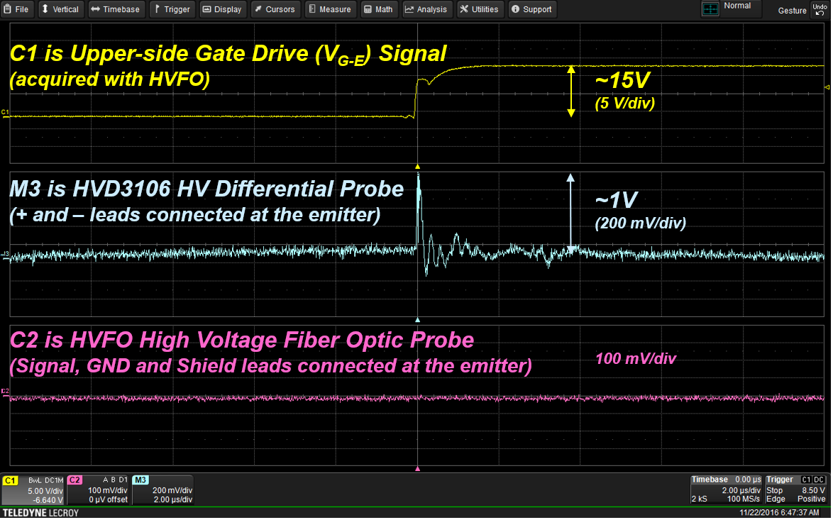
    For the positive half-cycle, the voltage spikes appear to be related the low-side switching. However, for the negative half-cycle, the voltage spikes appear to be related to the high-side switching. Based on the current loop, it seems most likely that this is an issue concerning common-mode rejection for the probe you are using. My best recommendation would be to use a better isolated probe, for example an optical isolated probe, if possible.

    You can test whether the voltage spikes are being introduced by the probe by connecting both leads of the probe to the HS ground (switch node), and if there is a voltage spike seen on the waveform, that would indicate the probe is the root cause for the spikes seen on the V_GS waveform. See the image below for an example:

    Best regards,

    Will