

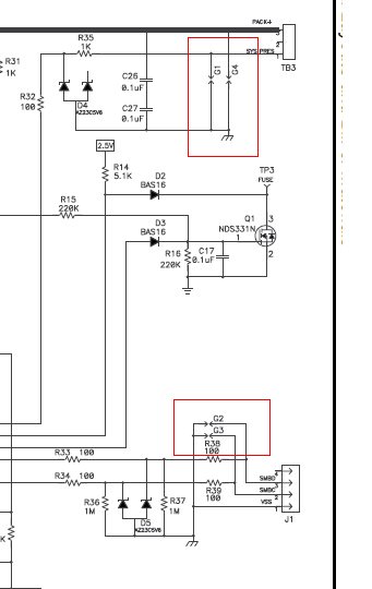
1. What does below marked(red) area, represent in z95 schematic:
2. While designing layout what should be recommended minimum distance two points: in SMBus connector, Cells connector (4P-1N)?
1. What does below marked(red) area, represent in z95 schematic:
2. While designing layout what should be recommended minimum distance two points: in SMBus connector, Cells connector (4P-1N)?
