This thread has been locked.

If you have a related question, please click the "Ask a related question" button in the top right corner. The newly created question will be automatically linked to this question.

LM25085 shutdown at ~16v

Other Parts Discussed in Thread: LM25085, LM25085A

Hello all,

I am seeking some advice on what might cause the problem described:

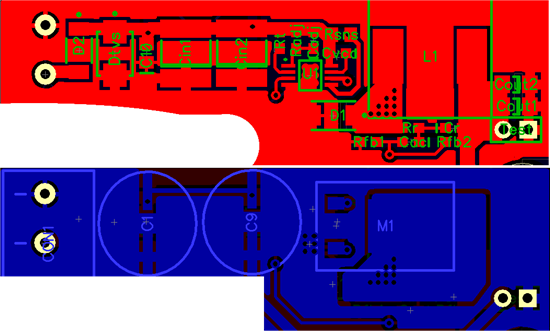
I am using a stock webbench design for lm25085, 5-40vin, 4vout @ 2amp, with low-op-ripple option.

When going to low-op-ripple, the IC is specified as the LM25085A version, but I only have LM25085. Hopefully I can still use the low-op-ripple circuit with that device?

Added a 20W 3R resistor to vout (to test load condition @ approx. 1.2amps). Then increased the input voltage from 5 volts upwards. At about 16.5volts, the vout shutsdown to zero. As soon as I reduce the vin below 16v, the vout comes back immediately. Nothing is getting hot! (Well, only the vout test-load resistor gets warm of course)

If I remove the load resistor, then I can run the LM25085 up to vin 30v and the vout is stable.

Any ideas what this could be? Based on the facts, I was thinking it could be the LM25085 going into shutdown mode at 16.5V... but why it would do that I am not sure? The Rt resistor is as specified at the webbench, 46K4. I am suspicious that because the webench changed my ic choice to the lm25085A type when it switches to low-op-ripple design, then perhaps the difference in feedback voltage (0.9v instead of 1.25v) means I need to change some values in the low-op-ripple components, and maybe they cause the problem?

I do have aTVS on the vin, specified to hold voltage at 26Vin. It might be faulty, but I think if that was kicking in, I would see a sharp rise in current consumption at the power supply... well anyway, before I start hacking the board apart it would be great to hear any other ideas what might cause this.

Thanks, Michael.

  • ... update...

    Found that the Rsns resistor was incorrect. A zero ohm had been installed in place of the 25 milliOhm. Now replaced that resistor, and the device (with a 10K load resistor, ~0.5Amp load) "shuts down" at ~10v instead of the previous 16v.

    Checked all the other components, and they appear correct.

    Is it likely that the LM25085 was damaged by the Rsns short? Or is that impossible, and I should I be looking elsewhere?

    Thank you.

  • well, the devices are the identical except for the internal reference: this means you have to change the resistor divider from VOUT to FB.

    looking at your description it seems to be related to the current information read on Rsense (noise, current ripple higher at high Vin).

    furthermore the big spread on IADJ an VCL_OFFSET don't help.

    to confirm this would be pretty simple: just increase RADJ (2 or 3 times its original value); while for the possible noise (possible because I have no clue about bom/schematic/layout of your application) I would just apply by default a little RGate (a 10R between IC and the PFET's gate).

    I'll wait for your FB.

    Vincenzo

  • Thank you for the suggestions Vincenzo!

    I will try these today and reply later.

    For reference, the R values I have now (specified by webench design) are:

    Rfb1: 4k87

    Rfb2: 11k5

    Rsns: 27.0 mOhm

    Rt: 46k4

    Radj: 2k21

    Rr: 24k9

    Other components:

    L1: 22uh, 43 mOhm,  4A.   BOURNS - SRR1260-220M

    Cr: 3.3nF,   Cac: 10nF

    D1: B360A-13-F

    Cin: 2x 10uF

    Cout: 47uF

    Cadj: 1nF

    Cvcc 1uF

    M1: FDD5614P

    U1: LM25085MYE

    And here is the pcb layout:

    I found an Excel spreadsheet at the LM25085 resources page, which seems to give different values to webench... although I notice its quite a bit older, so perhaps the webench vaues should be considered first?

    Anyhow.. if you see anything horrible with the pcb layout, that would be a great help to hear your advice.

    Thank you for your help, Michael.

  • Hello Vincenzo!

    I changed Radj from 2k21 to 4k42. I do not have something 3x available, but could series 2 resistors if you think its worth to test. However, doubling Radj did not appear to make any difference:

    At 12vin the vout drops to ~3.3v, at 13vin the vout drops to ~0.6v

    Perhaps some interference on Rsns is to blame.. perhaps layout related? Because of the layout, I am not sure I can insert 10R, but will go and try it.

    Are there any points on the pcb I should monitor with a scope to help identify the problem?

  • Small improvement...

    I moved D1 to the back of the PCB (same position, as fortunately there was space directly under it on the bottom side of pcb)

    Added 10nF at C9

    Isolated (cut around) the 6 vias on the bottom side of the pcb (which are connecting the LM25085 powerpad to the bottom of the pcb)- to ensure the D1 gnd does not pass directly into the powerpad.

    Now the vout is stable until ~15.5 vin. So a vin improvement of ~3.5 volts

    This might suggest the problem is with the pcb layout (ie. noise) ?? Within the current layout, are there another other modifications which might be made to test for improvement?

  • Bigger improvement...

    Added (between C1 and C9):

    10uf 50v ceramic (same as Cin)

    470pf ceramic

    Now the vout seems stable through the vin range 5 - 31vin

    vout is 4.25 @ 5vin, rising to 4.45vout @ 31vin

    load attached is 2R2, drawing 1.88 amps according to series multimeter. 

    However, I have made a fair few changes to the initial design, and would like to be certain which is/are the most likely factor?

    I read that the D1/Cin/Cout loop should be small, and considering I moved D1 to the back of the pcb, thought that the additional 10uF on the back would help provide that condition. Or is that a red-herring! Did the 470pF solve the case!

    Perhaps adding 2x10uF on back would now be better? Or removing 1 from the front, so I have 1 back, 1 front. Should I now revert the Radj back to the initial 2k21? I have still not fitted the series 10R to the PGATE (lack of space), but if that is needed / recommended when a Rsns resistor is used then I can add in the next revision. Probably too many questions... but for any part your advice would be much appreciated.

    Thank you!

  • well,

    there is some marginality in your layout.

    Please refer to the LM25085 EVM layout as reference or have a look at the attached applicaiton note.


    0121.Layout Guidelines for Switching Power Supplies.pdf


    7080.snva384a.pdf

  • Could you be more specific? not sure what you mean by "marginality".

    The generic switcher guidelines pdf looks interesting, thank you for posting.

    Otherwise, I can report that I changed the Radj back to the original 2k21 and removed the extra caps from the back of the board, except the 470pF, so it seems the solution for this design was to move D1 to the back of the board, and add a 470pF cap between D1-gnd and vin. On the next layout I will adjust the position of the FB resistor network, as it seems that might have been the culprit.

    Thank you for your helpful comments. 

    Michael.

  • yep,

    the layout exhibits many parasitic L (because vias, thin tracks, thermal relief, and so on...)

    these parasitic L are very dangerous and noisy in switching converters: best practice is to keep all the power components on the same plane, keep the compensation parts close to the IC and well "shielded" by GND copper; no thermal relief should be used, and so on...

    all these L times the current changes (dI/dt) caused by the switching, generate L x dI/dt undesired voltage spikes ==> high EMI problems, ringings, possibly ESD engagement (with failure and/or damages to the parts)

    for this purpose I asked you the 2 things:

    - change RADJ ==> since nothing changed in behavior it was a layout issue

    - apply RGATE ==> this will reduce the dI/dt of the above, reducing all the spikes as well

    The very little cap simply performs better than the 10uF at very high frequencies (the contents of the spikes) and, hopefully, seems to be enough to fix the problem...

    If I were you, I'll check the waveform on the swithcing node and see the spikes on it (you will need a fast DPO to properly observe them...)

    Vincenzo