This thread has been locked.

If you have a related question, please click the "Ask a related question" button in the top right corner. The newly created question will be automatically linked to this question.

TPS7H2140-SEP: Current limiting not working for our application

Part Number: TPS7H2140-SEP
Other Parts Discussed in Thread: TPS7H2140EVM,

Hi Experts,

Can you help with the inquiry below?

I'm using the TPS7H2140 to protect an RF amplifier from receiving damage during an over current condition. When I test the circuit with a resistive load, it works exactly as described in the datasheet. The output current is steady at the limit I have set (0.2A), and the output voltage browns out. When repeating the same test with the RF amplifiers as the load, however, the current limit never kicks in to protect them. The amplifiers have a bias voltage that I can change in order to alter the amount of current they pull through the TPS7H2140, and they are able to pull past 0.2A (I tested up to 0.3A) with no current limit kicking in. Probing the fault pin on the TPS7H2140 indicates that the part does not believe it is in an over current condition. Do you have an explanation for why the current limit only works with the resistive load, and not with the amplifier?

Regards,

Marvin

  • Hi Marvin,

    I have a few questions to help us debug what is happening.

    How are you measuring the load current that is being pulled from the TPS7H2140's output? Do you have any oscilloscope current probe waveforms? Have you measured the CS pin output to confirm what the device's current sensing capability is seeing? Can you share the RCS and RCL values you are using, or possibly your entire schematic to help us confirm how you have configured the part?

    Thanks,

    Sarah

  • Hi Sarah,

    Thank you for looking at this. 

    I have an update. The customer did some more testing and realized the issue isn't related to the load itself. What's actually going on here is that when current through TPS7H2140 is increased slowly, the trip level is much higher than the 200mA set point (the limit trips at 275mA instead). After the limit trips the current is clamped down to 200mA.

    I’m guessing most use cases for this part are a much higher current, so such a small difference in current limit setpoint vs actual trip point wouldn’t be significant. Unfortunately, it’s not ideal for our application. Could you explain specifically why this happens?

    Since we are sharing the output between the 4 channels on the device, technically the current limit is set to 50mA for channel 1. Would lifting the leads for channels 2-4 and setting the current limit to 200mA for the remaining channel have an effect on the trip point compared to the shared

    Regards,

    Marvin

  • Hi Sarah,

    More information:

    For this test, the customer is using the TPS7H2140EVM and swapped out the current limit resistors with one 40.2kΩ part (the limit is set to 50mA for 1 channel, all channels are sharing the load, so 200mA total). a current clamp connected to an oscilloscope at the output of the board is used to measure.

    The customer took the scope capture just to verify there were no unexpected spikes or problematic behaviors during the trip (which there weren’t). When the limit finally does trip at 275mA it then smoothly reduces to the set value (200mA) on the scope, and holds steady there.

    Can you please explain what determines the trip point itself? It would also be great to know if there is any way to reduce the gap between the trip point and the actual limit. For example if they were to disconnect channels 2-4 and change the current limit from 50mA for one channel to 200mA for one channel, would that have any impact on trip point?

    Also wanted to make it clear we are only seeing this gap between current limit trip and current limit set point when the load is dialed up slowly. When the EVAL board is powered on into an over current condition, the current is immediately limited to 200mA with no overshoot (in yellow below):

    Regards,

    Marvin

  • Hi Marvin,

    There is little information on using the device at such a small voltage. The datasheet only specs down to 250mA at a +/- 20% accuracy. Based on the 2 test conditions provided, it seems that the lower the current is, the larger the percentage of variance. But I'll look into this more this week and see if I can find more information that is closer to the customer's use case.

    I am curious to know if the results of their testing is affected by the thermal shutdown. Though I think it's unlikely at such a small voltage, it is possible that the 2 different behaviors are caused by thermal shutdown being activated. The customer can test by changing the THER pin as described in section 8.3.6.5.1.

    Thanks,
    Elizabeth

  • Hi Elizabeth,

    I would like to ask for an update. did you manage to looking into it more?

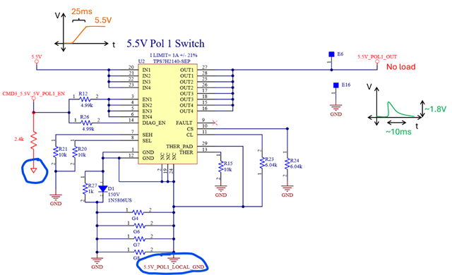
    The customer also had a different question today regarding the same part (the TPS7H2140). This time the switch is used in a different configuration; the schematic is shown below with the sketches of the input and output waveforms.

     These are the conditions:

    1. The enable (CMD3 below) is an active low, so the switch should be disabled.
    2. There is no load connected to the output.
    3. The input ramps on from 0 to 5.5V in ~25ms (orange curve sketched below).


    When the test is performed, the output spikes up to 1.8V before returning to 0V in about 10ms (green curve sketched).

    When a load is applied to the output (tested with a 15Ω resistor) there is no spike observed. During normal operation there should always be a load present, so fortunately this wont cause issues. If you can explain more about why this happens though, that would be great to understand for future reference.

    Regards,

    Marvin

  • Hi Marvin,

    I was unable to find any more information and also unable to find any more information that was closer to the customer's use case.

    I noticed in the schematic sent that the ground connects don't seem to be consistent for the part. There is a good chance that this is likely the cause of the odd behaviors from the part. Please make sure that the customer re-tests the part/circuit after they ensure that all connections to the device - pins, inputs, and outputs, such as the RF load - have a good common ground connection.
    Also of note regarding GND connections:

    Additionally, I noticed that the input and output lack bypass capacitors

    Please also confirm that the schematic sent is the same schematic for both inquiries.

    Thanks,
    Elizabeth

  • Hi Elizabeth,

    Thank you. 

    I noticed in the schematic sent that the ground connects don't seem to be consistent for the part. There is a good chance that this is likely the cause of the odd behaviors from the part. Please make sure that the customer re-tests the part/circuit after they ensure that all connections to the device - pins, inputs, and outputs, such as the RF load - have a good common ground connection.

    The GND network recommended in the datasheet (and included in the EVAL board TI provided) for inductive loads was followed. The original question was based on the EVAL module. That module offers the ability to short out the GND connection with a jumper, the customer wonder if that could be related to the problem but after testing with and without that jumper installed the results shows no difference in the current limit trip point.

    Ground network recommendation from the datasheet:

    Below is the ground network from the EVAL module schematic. “GND_IC” is the local ground in the case, and you can see they reference their current limit resistor to that net, but their current sense resistor to the larger GND plane.

    As for the second question about the spike on the output during input turn-on, the customer will run that test while shorting out the GND network but would like to understand why the GND network recommended by the datasheet would cause such a large spike (nearly 2V) on the output? The diode in that network selected has only a 0.2V forward drop. I’m not sure if you were looking at G4-G8 when you said the ground connects aren’t consistent, but those are not resistors, they are just a thermal path to get heat out from the local ground.

    Also, there is ceramic capacitance and tantalum capacitance as recommended by the datasheet on the input, it was not provided as it was on another schematic sheet.

    Regards,

    Marvin

  • Hi Marvin,

    I'll need some time to debug this. To reiterate and clarify: the customer is seeing the spike on the sent schematic but the slow current limiting on the EVM. Please confirm this is correct.

    Regarding my comment about the GND connections, I was specifically referring to the GND connections circled.

    The name 5.5V_POL1_LOCAL_GND seems to imply that it is connected to more than just what is on the given schematic rather than simply another net name like in our EVM. I was also curious if the other circled red GND connection has a good connection to the common GND for the circuit as it is unlabeled.

    I am also curious to know why all 4 channels are being used instead of just 1.

    Thanks,
    Elizabeth

  • Hi Marvin,

    Regarding the current limit, I have found an app note that is applicable for the TPS7H2140-SEP as it a "sister" part to TI's smart switch family: Adjustable Current Limit of Smart Power Switches (Rev. B)

    As described in section 4.1:
    The current limiting accuracy for TPSxHxxx devices is different between instantaneous over-current events and slow current creeping events. Current creeping is defined as a fault that results in the slow increment of load current from a normal operating level to the set current limit. In this linear region, the current limit ratio is not defined by the datasheet. The current limit meets datasheet specifications only when the FET is saturated by a fast increment of load current such as short circuit events, capacitor charging and inrush current clamping. A slow current creep keeps the FET in its linear region longer, causing a loss of current limit accuracy.

    Let me know when you have a response from the customer.

    Thanks,
    Elizabeth

  • Hi Elizabeth,

    I'll need some time to debug this. To reiterate and clarify: the customer is seeing the spike on the sent schematic but the slow current limiting on the EVM. Please confirm this is correct.

    That’s correct, current spike is from the schematic and slow current limiting is from the EVM.

    The name 5.5V_POL1_LOCAL_GND seems to imply that it is connected to more than just what is on the given schematic rather than simply another net name like in our EVM. I was also curious if the other circled red GND connection has a good connection to the common GND for the circuit as it is unlabeled.

    No, I see why having a net name might seem like the connection ties somewhere else, but it was labeled the net as a local GND for clarity to anyone else reading the schematic. The red GND circled is the general GND. The schematic sent is a rough draft of a revision so there are notes for a redline.

    I am also curious to know why all 4 channels are being used instead of just 1.

    All four channels are used to reduce power dissipation. In the case of the EVAL board example power dissipation is extremely low, but since a dedicated TPS7H2140 part will be required for a single output in the customer design, they just went ahead and used all four channels.

    Regards,

    Marvin

  • Hi Marvin,

    To answer the customer's second question, there is a very good chance that the spike in the no load condition is the result of current leakage:

    Let me know if the customer has any feedback or questions regarding this answer or my previous answer to the current limit.

    Thanks,
    Elizabeth