This thread has been locked.

If you have a related question, please click the "Ask a related question" button in the top right corner. The newly created question will be automatically linked to this question.

LMG3100R017: LMG3100R017 parallelization

Part Number: LMG3100R017
Other Parts Discussed in Thread: LMG3100EVM-089

Hi,
Two years ago, on this form page, regarding the parallel connection of GANs in a hard switching situation, it said, "In hard switching applications, we are still doing studies to understand the system requirements for paralleling this device with its integrated gate driver." Could I get an update on the current status?

In a full-bridge hard switching project, we are seeing burn-in failures in the high-side GANs, especially when we increase the input voltage (18–32V). 
Best regards.

  • Hello,

    We have designed a Paralleling board for LMG3100R017 and have tested out few conditions.

    Please refer to the below links for Board details and Test Results.

    Schematic and Layout guidelines for Paralleling LMG3100R017

    Test Results for LMG3100 Paralleling board

    Best Regards,

    Adithya Ankam

  • Hello,

    This is a great piece of work. Thanks for sharing.
    For the High Side power supply, an additional isolated power circuit is used instead of an internal circuit. I'm curious why external circuits are used instead of internal functions.

    Also, another thing I'm curious about is that the GAN shows the SRC pin and AGND connected internally.

    I couldn't access the layout files of the work you shared, but as far as I understand, in your work, they are drawn separately.

    They are combined on the LMG3100EVM-089 Evaluation Module board. Also, in the LMG3100R017 datasheet, Figures 6-1, 8-1, and 8-2 are separate, but Figure 8-3 is combined. Could you explain this in a little more detail?


    Best Regards,

  • Hello,

    Apologies for the delayed response here.

    I have gather all the information required to answer these questions.

    So to give you some background on the details,

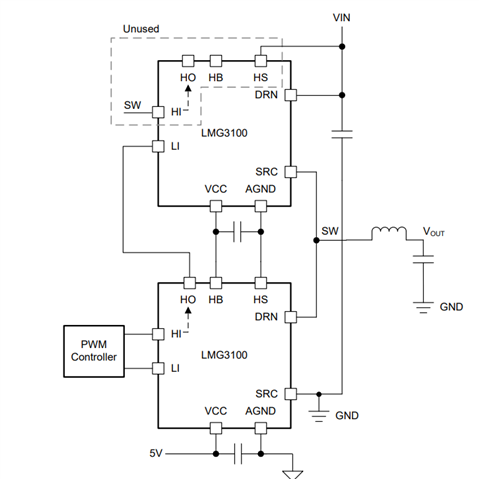
    There are 2 ways that can be used to provide PWM input to the TOP FET

    1.Using the internal level shifter to provide PWM to the Top FET using the HO of Bottom FET.

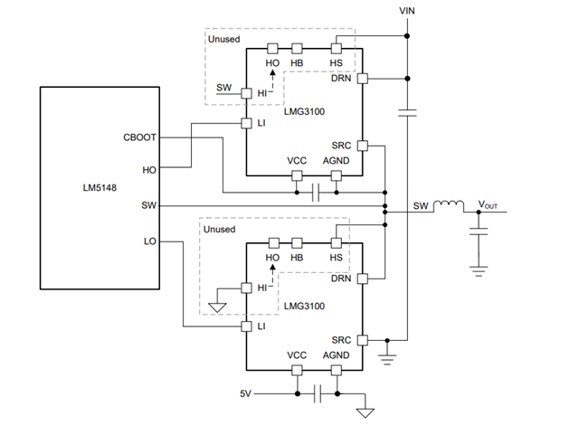
    2. Using external isolated circuit to provide PWM to the TOP FET- Similar to what we have in the paralleling board.

    We preferred method 2 in our board because method 1 will have a delay of typically 33ns added to the HI-> HO-> LI of Top FET -> Gate of TOP FET path compared to the LI Of bottom FET-> Bottom Gan.

    This extra delay becomes crucial in optimizing deadtime and hence we have given a isolated driver to provide the PWMs to the TOP FET.

    Yes our device internally has a connection between the AGND and SRC, please follow the guidelines for more details.

    I think this also explains the Datasheet figures as well.

    These are the older devices and we came up with newer generation devices which will be available from March 2026 where these internal delays are reduced and the internal level shifter circuit can be used without compromising on the Deadtimes and hence it is optimized.

    Regards,

    Adithya