This thread has been locked.

If you have a related question, please click the "Ask a related question" button in the top right corner. The newly created question will be automatically linked to this question.

BQ25750: buck boost problem

Part Number: BQ25750
Other Parts Discussed in Thread: BQ25756

Hi Team,

Following our previous discussion regarding automatic power-path switching, we have updated our design and are now using the BQ25750 instead of the BQ25756.

Our application is a battery-backup system. 

Expected operation:

  1. When a 24V adapter is present, the system should be powered from the adapter and VSYS should be approximately 24V.

  2. When the adapter is removed, the system should automatically switch to battery power.

  3. The battery voltage is approximately 28V, while the system requires a regulated 24V rail, therefore reverse buck-boost operation is required during battery-powered operation.

Current observations:

  • Adapter-to-battery switchover is working.

  • Reverse mode is enabled through I2C by setting EN_REV = 1.

  • REGN is present at approximately 4.9V.

  • PG changes state as expected when the adapter is removed.

However, we are facing an issue with reverse buck-boost operation.

Based on our understanding, the external buck-boost MOSFETs should be driven automatically when reverse mode is enabled. However, we do not observe the expected gate-drive behavior.

As a test, we connected SUP_DRV to REGN, which allowed the external MOSFET stage to become active and reverse power flow operation started.

The remaining issue is that although the reverse output voltage is configured to 21.4V, VSYS regulates at only approximately 17V.

Could you please help us understand:

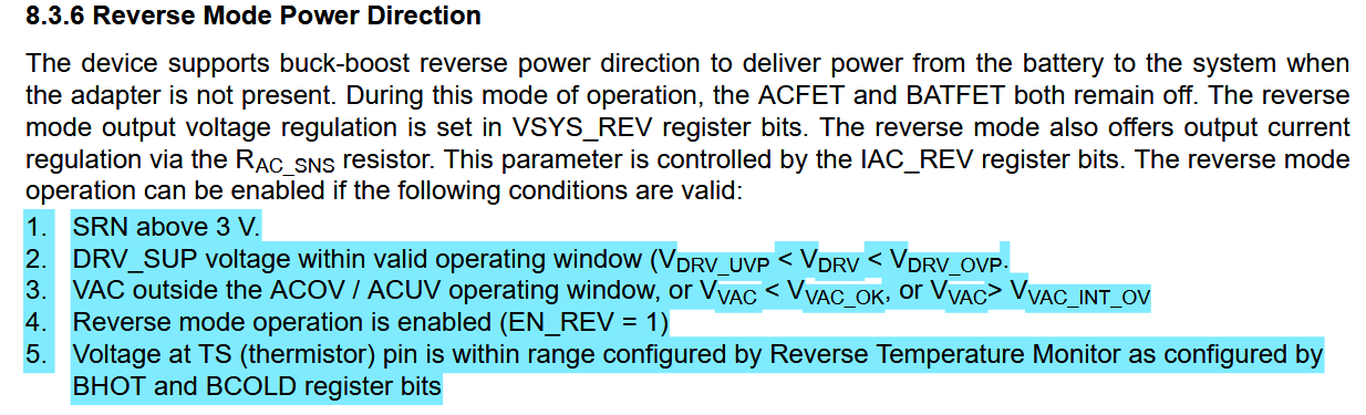
  1. What are the required conditions for proper reverse buck-boost operation in the BQ25750?

  2. Under what conditions should SUP_DRV be enabled?

  3. Is tying SUP_DRV to REGN an acceptable debugging method, or does it indicate a configuration or hardware issue?

  4. What could cause the reverse output voltage to regulate at approximately 17V instead of the programmed 21.4V?

  5. Which signals and register settings would you recommend checking to further debug this issue?

We can provide the schematic, register dump, and oscilloscope captures if needed.

Thank you for your support.

Hi Team,

Following our previous discussion regarding automatic power-path switching, we have updated our design and are now using the BQ25750 instead of the BQ25756.

Our application is a battery-backup system. 

Expected operation:

  1. When a 24V adapter is present, the system should be powered from the adapter and VSYS should be approximately 24V.

  2. When the adapter is removed, the system should automatically switch to battery power.

  3. The battery voltage is approximately 28V, while the system requires a regulated 24V rail, therefore reverse buck-boost operation is required during battery-powered operation.

Current observations:

  • Adapter-to-battery switchover is working.

  • Reverse mode is enabled through I2C by setting EN_REV = 1.

  • REGN is present at approximately 4.9V.

  • PG changes state as expected when the adapter is removed.

However, we are facing an issue with reverse buck-boost operation.

Based on our understanding, the external buck-boost MOSFETs should be driven automatically when reverse mode is enabled. However, we do not observe the expected gate-drive behavior.

As a test, we connected SUP_DRV to REGN, which allowed the external MOSFET stage to become active and reverse power flow operation started.

The remaining issue is that although the reverse output voltage is configured to 21.4V, VSYS regulates at only approximately 17V.

Could you please help us understand:

  1. What are the required conditions for proper reverse buck-boost operation in the BQ25750?

  2. Under what conditions should SUP_DRV be enabled?

  3. Is tying SUP_DRV to REGN an acceptable debugging method, or does it indicate a configuration or hardware issue?

  4. What could cause the reverse output voltage to regulate at approximately 17V instead of the programmed 21.4V?

  5. Which signals and register settings would you recommend checking to further debug this issue?

We can provide the schematic, register dump, and oscilloscope captures if needed.


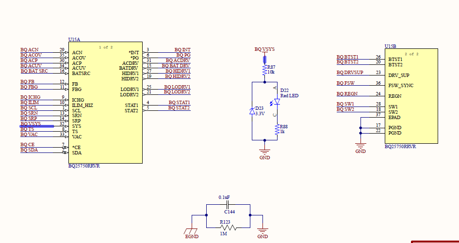
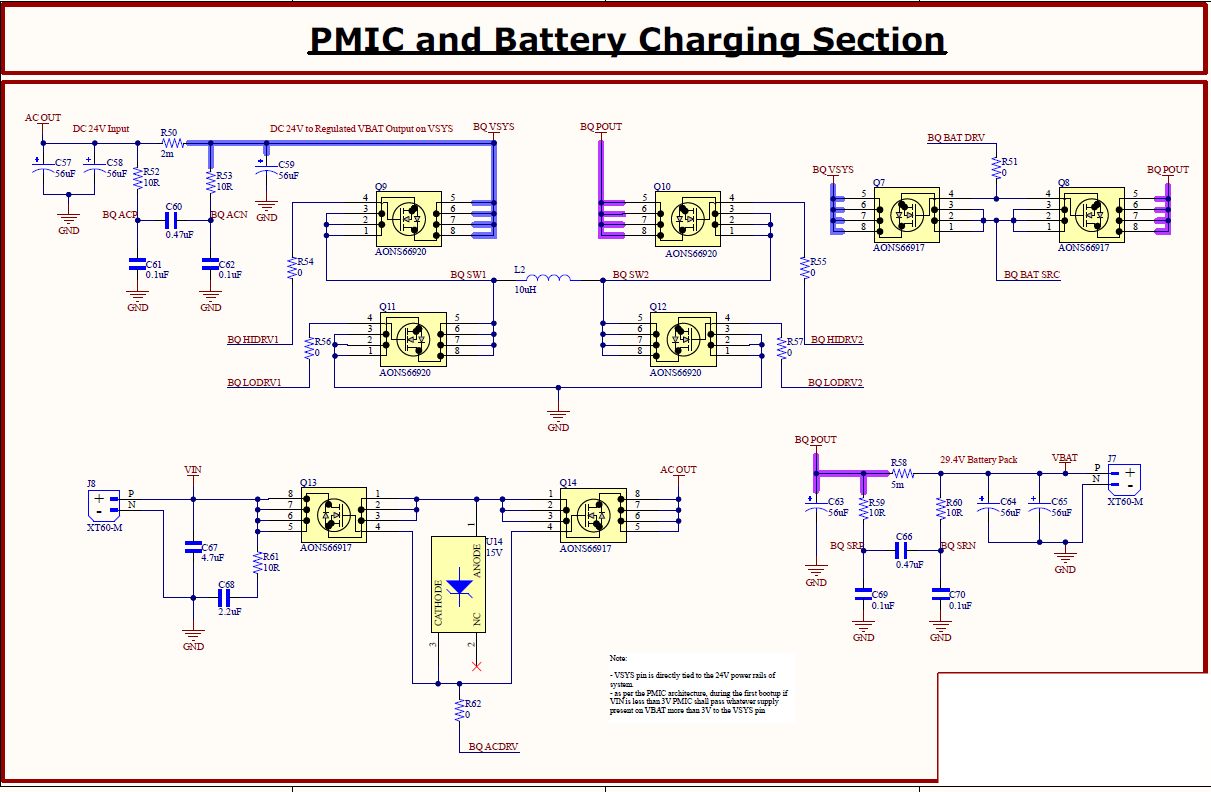
Below we are adding the screenshort of our schematic please review it.


img_20260525(1).pngimg_20260525(2).pngimg_20260525.png


Thanks and regards.
Druvit bhimani.


  • Hello Druvit,

    Thanks for working on this. Is this the same project as the questions asked in this other thread?  BQ25750: BQ25750 - Register writes to POWER_PATH_CTRL (0x19) not persisting, reverse mode fails to regulate VSYS 

    1. Here are the conditions required:

    2. DRV_SUP should be enabled whenever the charger is forward or reverse mode.

    3. Yes, this is an acceptable debugging method. Is DRV_SUP powered REGN or an external gate drive source in your schematic?

    4. What value is being set in the VSYS_REV register? Is the system writing the VSYS_REV register correctly?

    5. I would check the BQ25750 registers first. If the values are being set correctly, I would recommend looking at the SW1, SW2, VAC, and VBAT waveforms.

    The schematic looks good.

    Best Regards,
    Ethan Galloway

  • Hi Team,

    We have made further progress on the reverse mode operation.

    The reverse buck-boost operation is now working and VSYS is generated from the battery when the adapter is removed.

    However, we are facing a new issue when a load is connected to VSYS.

    System configuration:

    • Battery voltage: 28V

    • VSYS output: 24V

    • Load requirement: 24V, 5A

    Observed behavior:

    • Reverse mode starts correctly with no load or light load conditions.

    • When a 24V / 5A load is connected to VSYS, the buck-boost stage is unable to supply the required current.

    • During testing, the battery-side MOSFETs become excessively hot and eventually fail.

    Could you please help us understand:

    1. Does the BQ25750 support 24V to 24V reverse power delivery at approximately 5A load current in this configuration?

    2. Are there any reverse current limit settings that should be checked?

    3. What are the recommended external MOSFET specifications for this power level?

    4. Are there any specific gate-drive, inductor current, or switching node measurements that should be captured to determine why the battery MOSFETs are failing?

    5. Could this behavior indicate that the converter is operating outside its safe operating area or that the MOSFETs are not being driven correctly during reverse operation?

    We can provide the schematic, MOSFET part numbers, inductor specifications, register dump, and oscilloscope captures if required.

    Thank you for your support.

  • Hello Dhruvit,

    Thanks for the new information.

    I think the gate drive waveforms might be incorrect here. Can you send me the following information?

    • Can you send me the datasheet for the inductor and the BTST diode?
    • Can you check the SW1, SW2, VAC, and VBAT waveforms? If possible, it would also be helpful to check the inductor current waveform?
    • Can you also send me the layout? I want to check the layout to make sure there are no issues with the gate drive traces.
    1. Yes
    2. Can you read the registers to see if the IC is input current limit mode?
    3. The AONS66920 should work here. If you need more information, please see this application note: https://www.ti.com/jp/lit/an/sluaax9/sluaax9.pdf
    4. Can you check the SW1, SW2, VAC, and VBAT waveforms?
    5. See my above questions.

    Best Regards,
    Ethan Galloway

  • Hi TI Team,

    I would like to share the current status of our hardware and request your guidance on a few issues.

    System Configuration:

    • External supply: 24 V

    • Battery voltage (fully charged): 29 V

    • Load: 24 V

    Initially, we were facing a battery charging issue. To resolve this, we made a hardware modification by connecting a jumper between the CE pin and GND without changing any other components. After this modification, the charging issue was resolved.

    Current Status:

    • Battery charging is working properly.

    • Automatic switching between the external supply and battery is working correctly.

    • Reverse mode also works correctly once it is activated.

    Issue 1: Reverse Mode at Initial Battery Connection

    When only the battery is connected during power-up, the BQ25750 does not enter reverse mode automatically. However, after resetting the MCU, reverse mode is triggered successfully. Once reverse mode has been enabled after the MCU reset, all subsequent switching between the external supply and battery works correctly, including reverse mode operation.

    Could you please advise why reverse mode does not start automatically during the initial battery connection and whether any additional initialization sequence or register configuration is required?

    Issue 2: ACUV/ACOV Resistor Modification

    Due to the characteristics of our external power source, we modified the ACUV and ACOV resistor divider values as follows:

    • R85: Changed from 133 kΩ to 4.7 kΩ

    • R86: Changed from 25.5 kΩ to 47 kΩ

    The intention was to set the input undervoltage and overvoltage detection window approximately between 22 V and 26 V.

    After making this hardware change, battery charging no longer works correctly.

    Could you please confirm whether these resistor changes require corresponding firmware changes, such as updating the ACUV/ACOV threshold registers or any other configuration registers in the BQ25750?

    Issue 3: MOSFET Damage During Slow Input Voltage Ramp

    We observed another issue during testing.

    Test conditions:

    • The system is initially powered only by the battery.

    • The external supply voltage is then increased slowly from 0 V to 24 V.

    During this slow voltage ramp, the following MOSFETs are damaged:

    • Q8 (BATDRV MOSFET)

    • Q10

    • Q12 (Buck-Boost MOSFET)

    Could you please help us understand the possible reason for this failure? Is there any recommended startup sequence, gate drive consideration, or hardware modification to prevent these MOSFETs from being damaged during a slow input voltage ramp?

    For reference, you may refer to the schematic that I uploaded in the previous discussion thread.

    Thank you for your support. We appreciate any suggestions or recommendations.

  • Hello Dhruvit,

    Could you please advise why reverse mode does not start automatically during the initial battery connection and whether any additional initialization sequence or register configuration is required?

    I think the reverse mode commands aren't being written to the BQ25750 here. Can you check if the BQ25750's register show that reverse mode has enabled? You may need to add a wait time to the reverse mode I2C commands. This will let both the BQ25750 and MCU power-up and the voltages to settle.

    Could you please confirm whether these resistor changes require corresponding firmware changes, such as updating the ACUV/ACOV threshold registers or any other configuration registers in the BQ25750?

    These shouldn't require any changes. Did you check the resistor settings with the design calculator or the ACUV/ACOV FAQ?

    Could you please help us understand the possible reason for this failure? Is there any recommended startup sequence, gate drive consideration, or hardware modification to prevent these MOSFETs from being damaged during a slow input voltage ramp?

    Can you capture the VAC, BATDRV, VBAT, and SW1 waveforms on an oscilloscope? This will show us if the BATDRV voltage is oscillating ON and OFF. This can happen if the input supply is dropping below ACUV when charging starts.

    Best Regards,
    Ethan Galloway