This thread has been locked.

If you have a related question, please click the "Ask a related question" button in the top right corner. The newly created question will be automatically linked to this question.

Ripple on TPS56221

Other Parts Discussed in Thread: TPS56221

Hi,

I have implemented a power solution based on TPS56221.  The schematics is detailed on the following document simulated under switcher pro. 2514.U94_1V_22A.pdf

On my board, I powered a processors. The processor is on stand by mode for the moment (less than 1A is provided by the power supply)

I observe the following signal :

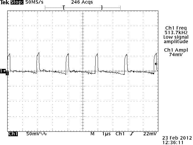
I see the switching frequency (500KHz).

I have a ripple of 50-60mV.

How can reduced this ripple ? I have tried to decreased and increase the number of output capacitor but the result is identical.

Could you give me some ideas to reduce the ripple ?

Best regards,

Laurent.

  • Laurent,

    Thank you for your interest in TI parts.

    The schematic you posted is directly from SwitcherPro. Is your schematic exactly the same? Are you using the same or equivalent parts on your BOM?

    Can I ask you to post your actual schematic, BOM and layout so I can get a better idea?

    Thanks,

    MC.

  • Martin,

    Thank you for your reactivity.

    Please find below schematics, bom and layout of the concerned part.

    6735.Power_Supply_Schematics.pdf

    3365.Layout_Part.pdf

    My schematics seems the same as switcher pro schematics.

    Best regards,

    Laurent


  • Laurent,

    How and where are you measuring the ripple? How long are the scope leads?

    I see that most of the power component placement is good, but the return, or ground side of the output caps is far away from the input bank. Keep in mind that the AC current in the choke flows through the output caps, and the current must return from the ground side of the output caps back to the ground side of the input caps during the ON time, and to the low side FET source during the OFF time. You have an incredible amount of copper, more than most designs can afford, but the distance is quite long at 500kHz.

    The shape of the output ripple is mostly resistive, plus inductive (which may be being masked buy the BW limiting) rather than capacitive. Your output cap bank is purely ceramic, which should provide a ripple signature more like a full wave rectified sinusoid (comes from the integral of a low duty cycle sawtooth). So your layout is adding inductance and resistance to the filter impedance. This inductance and resistance are added by the distance and the vias. Both despite the incredible amount of copper. Ideally you would want the output caps right beside the input caps so that the return current path is very short and the entire high current, high frequency AC loop is very small. That would keep the generation of ripple voltage to a minimum, and the DC output current you can bus to the load usually without issue other than voltage drop. But bussing the DC current does not introduce noise or ripple. The AC current in the input and output filters needs to be contained in very small groups and very small loops. I would also move the choke closer to the 56221 and reduce the size of the SW Node copper to a bare minimum.

    I checked the inductor specs and the device is good to about 30A, so certainly you are not saturating.

    So the ripple data you provided might be related to how and where you are measuring it, but more likely due to the placement of output caps wrt input caps.

    What you can try for a test is to solder your output bank return end-caps to the copper near C928, and have them tombstoned. Also tombstone the choke but flip it around so that its underside faces right (in your layout picture) and make a very short connection between the flying choke lead and the flying cap end-caps. Then bus the DC voltage back out to the Vout copper at the via farm. Measure the ripple right across one of the tombstoned output caps. This sounds like a lot of work, but it may give you the results you are looking for.

    MC.

  • Martin,

    Thanks a lot for your answer. I try your idea and the ripple has decreased. Now, I measured a ripple less than 5mV. Then, the distance between output capacitors and input capacitors were too long.

    Now, Im' going to do a layout modifications to implement this solution.

    You have solved my trouble, then we can close this request.

    Thanks a lot,

    Best regards,

    Laurent