This thread has been locked.

If you have a related question, please click the "Ask a related question" button in the top right corner. The newly created question will be automatically linked to this question.

why i can't get output in TPS65070

Other Parts Discussed in Thread: TPS54331, OMAP-L138, TPS65070

Hello Forum

In my TPS65070 design I plan to power the TPS65070 from a 7.4V source via a DC/DC converter(TPS54331). This DC/DC converter output can be set to 5V and can Supports up to 3A continuous output current. The TPS65070 in my design is power for OMAP-L138. the figure below is my design of TPS65070. now I meet problem.


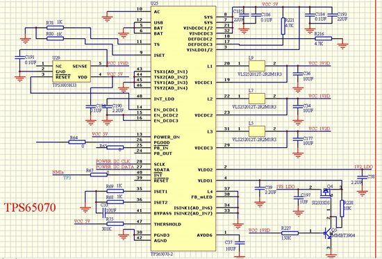
1/  I measure the VCC_5V, is 4.996V, so is correct.

2/  the output of DCDC1,DCDC2,DCDC3 is nothing, the value that measured by my multimeter is 3.6mV(DCDC1), 1.8mV(DCDC2), 9.9mV(DCDC3),

3/  the output value of LDO1,LDO2 is 0.83v(LDO1) , 1.09V(LDO2)

So I want to know why it can be this. Is that my design wrong?

( From another post I understand that, with the input voltage applied to SYS, I should connect the AC, USB and BAT inputs to GND; connect TS to GND through a 1kohm resistor; and connect ISET to GND through a 1k resistor, PB_IN can float (has internal pull-up) and POWER_ON should be connected to SYS )

By the way, I find a phenomena that when I connect the PB_IN to GND, the input voltage of VCC_5V will be pull down to 2.24V. why?

Your responses would be much appreciated!
Thanks

XUNLIANG

  • also, i measure that the THRESHOLD pin of TPS65070 is 1.04V, and the RESET pin of  TPS65070 is 840mV, so the problem is that, why the signal "RESET " is abnormality?  in the page 33 of DATASHEET of TPS65070, it can be see that if the voltage of the THRESHOLD pin is above 1V, the output pin RESET will goes high ,but what's the normal value of the RESET pin?

  • Hello Xunliang,

    There may be an issue with how the inputs source is connected. The SYS pin is considered an output and not an input. Instead, AC, USB, or VBAT are inputs to the TPS65070. Since these are grounded in your schematic, the IC thinks it is off or is in UVLO and none of the internal circuits are on. I recommend moving your input 5V source to the AC input and possibily open circuiting the USB and VBAT pins.

    Regards,

    Darwin

  • Below is an app note that discusses using the TPS65070 to power OMAP-L138 for your reference.

    http://www.ti.com/lit/an/slva371b/slva371b.pdf

  • Thank you Darwin

        but i have confirm form that the pin SYS can be  powered directly by 5V in other post(see this post: CAN TPS65070 VDCDC1 and VDCDC2 connect together for larger output power on 3.3V?),  he said "The SYS pin can be powered directly even though it is classified as an output." ,so am i understand wrong?

  • From  another post i know that if the pin AC is not used ,it should connect  a 1uF capacitor to GND, and if USB is not  used , it should connect to GND, if BAT is not used, it should connect  a 10uF ceramic capacitor to GND, so i have these questions :

    1/  if i not use BAT and AC and USB , how these pins connect? connect to GND directly? or connect a capacitor to GND?

    2/  does pin BAT and AC and USB not use  and pin  SYS be powered  by 5V  directly? i do that and find  it doesn't work, which can be seen above, so i doubt it.

    3/  i connect 5V to AC pin and connect pin BAT to GND by a 10uF  capacitor and connect pin USB to GND directly, the pin SYS  is connect to VINDCDC1/2, VINDCDC3 and VINLDO1/2 as the datasheet said, the other pins connect as the figure above , but i find that the output voltage of DCDC2 and DCDC3 is 1.15V, and the LDO has no voltage output , so does the LDO has enable pin? why it  can't output? and why does the DCDC output wrong?

    4/  i even doubt my chip of TPS65070 is a bad one, or a bogus one , can you give me the appearance of the chip of TPS65070 as a  reference?

    thanks!

  • Hello Xunliang,

    Thanks for your update. I have tested a similar circuit using the TPS65072EVM. Yes, you can place a voltage source at SYS as an input voltage for the converters. From your schematic, ENDCDC2 and ENDCDC3 are connected to ground. On page 54 of the datasheet, the table shows that the EN pins must be connected high when enabling the converters manually or enableing the associated bit. After I pulled the EN pins high, I gained control of the converters with the I2C control. For resistors 216 and 221, can you short themso that you get a HIGH on DEF3 and LOW on DEF2 as see if that changes the output voltage slightly? Lastly, please confirm that the input power supply is current limited to the appropriate current. I believe the input voltage may be drooping when you turn on the device (pull PB_IN low) because the input power supply is current limiting.

    To answer the above questions:

    1) and 2) Please follow the design notes that you stated previously when they are not being used. That is, AC with 1uF to GND. USB grounded. BAT with 10uF to GND.

    3) The LDO does not have an external enable pin. You must configure the internal registers via I2C to turn it off or on. By default, the ENLDO is ON. I do not see this issue on the EVM. Please check your registers to see how they are configured while your are operating the device. That way, you can see if your LDO is not working properly or just off. This also goesfor the DCDC outputs as well. I recommend purchasing the TPS65070EVM because it comes with software that allows you to see the bits for each register and configure them as you want..

    4) If you feel that your IC may be bogus. Please order samples from TI.com or purchase the EVM fromthe TI eastore for your reference. The top marking on the ICs should be "TPS65070 TI ##L LLLL G4" where # = numbers and L=letters.

  • Thank you for your reply

    But I still have questions about your standpoint, look at this figure below, is the page33-34 of datasheet.


    I am confused about how to connect the enable pins, as the OMAP-L138 in my design is powered by TPS65070 and can’t write the registers in TPS65070 before it startup, so I hope TPS65070 can output default value when it launched.

    After read the figure above, I think that it has two enable sequencing modes in it, one is enabled by EN pins, and the other is by registers. In the first mode, which can control converters independently, the EN pins should set to high and DCDC_SQ[2,0] in register CON_CTRL1 should be 101; in the second mode(automatic internal sequencing) the EN pins are ignored and should be set to low, Bits DCDC_SQ[2,0] define the sequence of DCDC converters. as the default value of Bits DCDC_SQ[2,0] is 011 for TPS65070, so if I set EN pins to GND and .place the 5V source to SYS, the DCDCx will output corresponding voltage ..

    So :

    1/  Am I understand it right? If not, how can I understand the figure?

    2/  the EN_DCDC2 and EN_DCDC3 in the schematic of OMAP-L138 EVM is connect to GND, so it sequenced in second mode as I said?

    3/  I can sure that the input power supply is not current limiting, and the input voltage is not drooping when i turn on the device. If I place a voltage source at SYS, I keep the PB_IN floating and pull up the POWER_ON by a resistor, and do not need to pull PB_IN down to start the chip, right?

  • Hi Xunliang,

    I'm sorry for the confusion, I thought you were controlling everything through I2C bus. I hope this will clarify everything:

    For turning on the device, you must still push PB_IN low in order to turn on the converters and its okay to have POWER_ON signal high while having PB_IN low. That is, PB_IN low, POWER_ON high, then release PB_IN. The sequencing of the converters is based on the default on Table 9 of the datasheet and explained on page 53. This says DCDC3 turns on, then DCDC2 while DCDC1 is externally controlled. This is why ENDCDC2 and ENDCDC3 should be connected to ground, and ENDCDC1 externally controlled.

    For powering down , you must pull POWER_ON low to turn the converters off.

    Regards,

    Darwin

  • Hello Darwin

    Thank you for your Patient reply !

    But may be you have misunderstanding my ideas, I know the chip should be launched by “PB_IN low, POWER_ON high, then release PB_IN”, I want to know how it sequencing when i start it. Now, simply to say,

    1/  if I pull up EN pins, the launch steps(PB_IN low, POWER_ON high, then release PB_IN) will be no use and DCDC converters will be work all along, right?

    2/  I attempt to connect EN_DCDC2 and EN_DCDC3 to GND, and connect EN_DCDC1 to 5V, but find no outputs after launch steps(PB_IN low, POWER_ON high, then release PB_IN),why?

    Regards

    xunliang

  • Hello Xunliang,

    The output voltages work differently when the input voltage is either on (AC or USB) or (SYS or BAT).

    1. If you pull-up EN pins:

    If VIN is on SYS or BAT - you must still push PB_IN low, POWER_ON high, release PB_IN. For the TPS65070, DCDC2 and DCDC3 will turn on regardless of EN2 or EN3, while DCDC1 depends on EN1 which for 1. is pulled up so it will be on.

    If VIN is on AC or USB - you can either do (PB_IN low, POWER_ON high, release PB_IN) or you can just pull POWER_ON high. For the TPS65070, DCDC2 and DCDC3 will turn on regardless of EN2 or EN3, while DCDC1 depends on EN1 which for 1. is pulled up so it will be on.

    2. This sequence should turn on the power supplies whether VIN is on SYS or BAT or AC or USB. This leads me to believe it may something else in your circuit. Did you end up making the changes on how USB, AC, and BAT must be terminated. Also, for SCLK and SDAT, how is this terminated? What is "power dc clk" and "power dc data"?

  • Thank you Darwin!

    Now my chip was worked after i changed my chip, and i find that the pin BAT should be connect a capacitance to GND when power the chip on SYS, and pin AC and USB can be floating or connect to GND directly.

    and thanks for your reply again!

    regards

    xunliang