This thread has been locked.

If you have a related question, please click the "Ask a related question" button in the top right corner. The newly created question will be automatically linked to this question.

Low-Frequency Noise at SEPIC Output (using LM3478)

Other Parts Discussed in Thread: LM3478, LM3481, LM3488

Hello

My design comprises a SEPIC stage with 4V5-20V input range and 13.5V output at max. 1A. In most cases the load is significantly lighter, coming down to a 0.5W minimum instead of 13.5W.

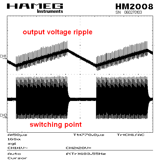
In these conditions there is a strange regulation behaviour seen for higher input voltages. Everything is fine for Vin below 16V. At about 16V5 the regulation gets jumpy with noise in the lower kHz-range. Furthermore, the average output voltage rises to 14.5V, meaning, that the feedback input is almost permanently above 1.25V (a voltmeter reads 1.30V average).

I varied in large scales the capacitor at the feedback pin (usually 100pF to GND) and the capacitor-resistor series from COMP to GND, all to no avail. The scene does change as soon as the load increases a little. However: the total load is controlled by uController (turning on/off parts of  the circuit) and is always kept at minimum.

Compare the two images in the attached file with 12V input (everything OK) and 18V (with 2kHz ON/OFF alternation).

7268.LM3478 Sepic Stage.pdf

Where do I have to look at to make this (or a similar) design stable for light loads?

Thanks and regards

Thomas

  • Hello Thomas,

    I am the apps engineer for this part. I will look into it and I will let you know as soon as possible.


    Regards,

    Giuseppe

  • Hello Giuseppe

    the Capacitor 100pF from FB to GND does indeed disturb a little. Removing it entirely or connecting it instead from FB to Vout changes the behavior a bit. The onset of the oscillation is shifted to a slightly higher input voltage, but it still begins oscillating well below 17V input.

    I concluded that I did not find the proper cure.

    Regards, Thomas 

  • I will build the same circuit in order to verify the behavior, in the meantime could you please provide me waveforms of switching point and output voltage ripple when the problem occurs?

    I am not sure but it seems like over voltage protection. OVP is sensed at the feedback pin and will cause the mosfet to turn off. With the mosfet off, the output voltage will drop. The LM3478 will begin switching again when the feedback voltage reaches Vfb+(Vovp - Vovp(hys)) (see the datasheet for detail).

    By looking at the switching point there will be some skipped pulses and by changing the amount of output capacitance you will also change the frequency of the ripple.


    Regards,

    Giuseppe

  • I'm a bit lost, Giuseppe.

    In the file there are the waveforms of which you speak. Do you need them with another resolution, e.g. 1usec/div? Then we do not see the whole picture. Waveform of switching point: is that the Gate Drive?

    Regards, Thomas

  • Hi Thomas,

    I have a thought, to me it looks like you are running into minimum on time issues. From your 15k resistor on FA/SD I am guessing your switching frequency is about 850 kHz. With a 325 ns typical minimum on time you can expect it to start pulse skipping at 28% duty cycle. When you are operating in DCM the duty cycle will decrease with your load current. It also makes sense you will see it occuring more at higher input voltages because the duty cycle will be lower then. The estimated duty cycle in the 18 V input, 60 mA your provided should be 26% duty cycle.

    One scope shot that may help as he mentioned is a zoom in of the switching point to measure the on time. I believe he is referring to the node between the input inductor, the switch and the series capacitor.

    Regards,
    Anthony 

  • Hello Thomas,


    the images you sent me are about the feedback voltage and the output voltage, in order to understand the problem i'd like to take a look at the switching waveform across the mosfet drain to ground and the output voltage ripple.

    As I said before i am pretty sure that the LM3478 is bursting and the circuits is working in OVP mode since the load current is very low.

    I don't really think it's a minimun on time problem. The duty cycle for a SEPIC converter is defined as D = Vo / (Vi + Vo).

    D = 40% when Vin = 20V --> ton = D/fs = 0.4/800e3 = 500ns

    D = 75% when Vin = 4.5V --> ton = D/fs = 0.75/800e3 = 937ns


    Regards,

    Giuseppe

  • I have the same problem. My circuit is designed to use 5-30V in and 24V out, 1A max. Switching frequency is about 350 kHz. The inductors are coupled, 2x10uH. Input cap is 10uF, coupling cap is 10uF, and output caps are 2x10uF.

    At medium to high loads, or light loads with input is below 18V, everything works fine.

    However, at light loads with an input of 18V or more, the current drawn from the input isn't stable. The inductor is making an audible noise of a few kHz. Scope signals are almost identical to the ones Thomas has attached to his opening post.

    It seems like the duty cycle is a bit too high, and the IC isn't compensating for it. The output voltage is constantly rising. When it reaches a threshold, the gate is turned completely off. It will remain off for about 100 micro seconds, then it starts over again. The higher the input voltage, the faster the output cap will reach the threshold.

    I have been trying different compensation networks, but it doesn't seem to change things much. By following Application Note 1484, I calculated Rcomp 270 ohm and Ccomp1 2.2uF.  With these values it will remain stable up to 19V instead of 18V, which has been the case with various other values.

    If I put a 1000uF electrolytic cap at the output, the behaviour is the same, although the frequency gets a lot lower because of the slower charge time.

    Is there a solution to this?

    I can attach schematic and scope pics if there is interest.

  • Hello Nyman,


    it seems to me that the LM3478 is working in OVP mode and it is bursting (overvoltagep protection mode). When I say bursting I mean there is not a continuous operation because the part stops switching when the output voltage hits a certain value (please see the datasheet for more details and take a look at the previous posts).

    Could you please provide me the schematic and waveforms about the switching node (drain of the mosfet to GND) and the output voltage?


    Regards,

    Giuseppe

  • Hello,

    attached is the schematic as well as some measurements at 15, 20, 25, 30V input, and 24V output with 360 ohm load.

    7762.LM3478_measurements.zip

  • Hello Nyman.


    the part is working on OVP mode as expected. In a previous post I wrote the following:

    OVP is sensed at the feedback pin and will cause the mosfet to turn off. With the mosfet off, the output voltage will drop. The LM3478 will begin switching again when the feedback voltage reaches Vfb+(Vovp - Vovp(hys)) (see the datasheet for detail). By looking at the switching point there will be some skipped pulses and by changing the amount of output capacitance you will also change the frequency of the ripple.

    LM3478 is working in OVP mode and it is bursting (overvoltagep protection mode). When I say bursting I mean there is not a continuous operation because the part stops switching when the output voltage hits a certain value.

    You can verify what i just wrote from the waveforms you sent me:

    This is a normal behavior and it is implemented in order to increase the efficiency at light load.

    If the efficiency at light load is not a problem you could decrease the feedback resistor values such to generate a dump load which keeps the switching action of the LM3478.

    For instance if the top feedback resistor is 100K and the bottom feedback resistor is 10K you could use 10K for the top and 1K for the bottom. Keep decreasing until you get the desired ripple, anyway you are going to lose in terms of efficiency.

  • I can accept that. But I think we might change the IC, because the noise isn't very pleasing to listen to. I didn't expect this to be normal. The first thing I did when I found this thread was to search through the datasheet for the word "burst". The word wasn't in the datasheet,  and I couldn't find anything similar on the list of features in the first page. I just read the datasheet again to see where it is mentioned, and found this:

    Under extremely light-load or no-load
    conditions, the energy delivered to the output capacitor when
    the external MOSFET in on during the blanking interval is
    more than what is delivered to the load. An over-voltage comparator
    inside the LM3478 prevents the output voltage from
    rising under these conditions.

    I didn't pay any attention to this when I read through the datasheet the first time. I suspect that was because of the words used; "extremely light-load or no-load
    conditions". I would interpret that as a load of a few mW. In my case, I have a (dummy) load of 1.6W (two 180R power resistors in series), and it's still bursting. I wouldn't call that an "extremely light load".

  • Sorry to hear that, anyway before to move on another IC please try the following.


    1. increase the inductance, the converter will enter DCM with a lower output curren value and it will increase the duty cycle in DCM

    2. change the output capacitor, it will change the frequency of the low frequency ripple, it could move out from the audible region

    3. increase the switching frequency, the problem is caused by the minimum on time of the LM3478, the duty cycle in DCM is D =sqrt[( Vout/Vin -1 )*(2*L*Iout*fsw/Vi)] hence, by increasing the switching frequency you increase the duty cycle in DCM


    If that does not work, i would suggest you to use the LM3481.

    Hope that solves the problem.

    Regards,

    Giuseppe


  • I am having a very similar problem.  When the load is only a few watts the switching is generating to much output and the voltage goes up.  My supply is in an embedded device that has several PWM devices on the 12V and some low power sensors.  When the PWM devices are off the sensors are getting this 12V- 13V saw tooth voltage.  The voltage fluctuations is trouble for the sensor analog circuits.  I can deal with some minor voltage fluctuations but a whole volt is bad.

    Question Why does increasing the switching frequency help?  I would expect lowering the frequency to help.  The min FET on time is controlling the duty cycle so if I lower the switching frequency I would lower the FET's duty cycle.  Am I missing something?

  • Hello,

    The OVP and min on time behavior is the basic operation of the LM3481, LM3478, and the LM3488. Have you experimented with a higher inductance value? If you can allow a minimum load, then you can go away from the oscillatory behavior at the expense of efficiency. But as such anything else you do will just move the DCM behavior at different operating points. 

    Regards,
    Akshay

  • Hello,

    Thanks for your answer. I will try it tomorrow.

    As far as I understood from the datasheet, there is a hysteresis and also a treshold voltage over the OVP voltage of 1.4V. This treshold + hysteresis voltage sum up to around 120mV ptp around the 1.4V feedback voltage. It is about +/-4% which means +/-0.88V around my 22V output voltage. How exactly would this change of inductance solve the problem? It is a problem of thresholds which are already set into those chips.

    I saw that in some datasheets they offer this solution:

      Do you think it can help?

  • Why did you erase my question and my post?

  • I did not erase it. I split it from this thread and replied. I am surprised you did not get an email regarding that. Here it is: http://e2e.ti.com/support/power_management/non-isolated_dcdc/f/196/t/345752.aspx

  • Just got the E-mail now... about an hour later...