This thread has been locked.

If you have a related question, please click the "Ask a related question" button in the top right corner. The newly created question will be automatically linked to this question.

LMZ10501 abnormal behaviour, Temperature above 60°C

Other Parts Discussed in Thread: LMZ10501

Hello,

we are using the LMZ10501 as a power source for two different designes (5V --> 1V, 5V --> 3.3V). At first everything went perfect and there were no issues. But until today 3 boards (2 of the first and 1 of the second design) started to get issues regarding the LMZ10501.

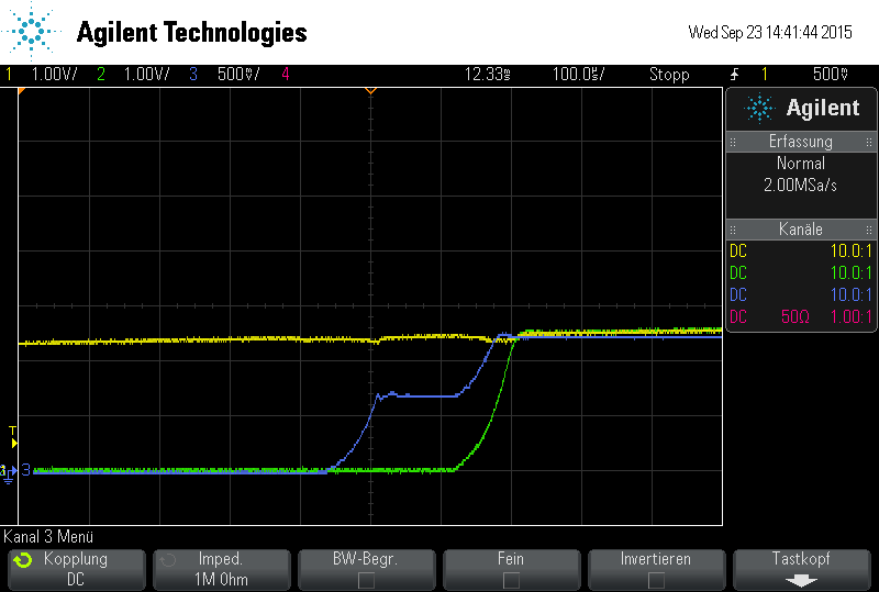
The power consumption of one of the design is around 120mA @ 3.3V, which should be no issue at all. The output voltage is still stable @3.3V but the overall power consumption of the board went from 110mA @ 5V to 250mA @ 5V and the LMZ10501 becomes very hot --> 60°C+ (25°C ambient). So the system is still working but the LMZ10501 should be a risk with higher ambient temeratures. 

I did some research on problematic boards and found out that the enable pin (1) works differently than a working board. The pin is left floating so i can use a voltage to disable the LMZ10501. After applying 0V to the pin the output voltage is correctly disabled BUT the overall power consumption of the board is still nearly the same and the LMZ10501 is still very hot. After removing the voltage from the pin the output voltage is still disabled! That is an abnormal behaviour because it should start working again as i can see it on a working board. The only way to enable the output voltage again is by applying a voltage again. It is hard to tell which voltage because it differs everytime (somewhere between 2V-5V). After applying the voltage to the enable pin the ic is working again and i can remove the voltage.

Do you have any idea, help or advice?

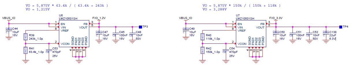
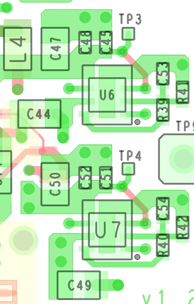
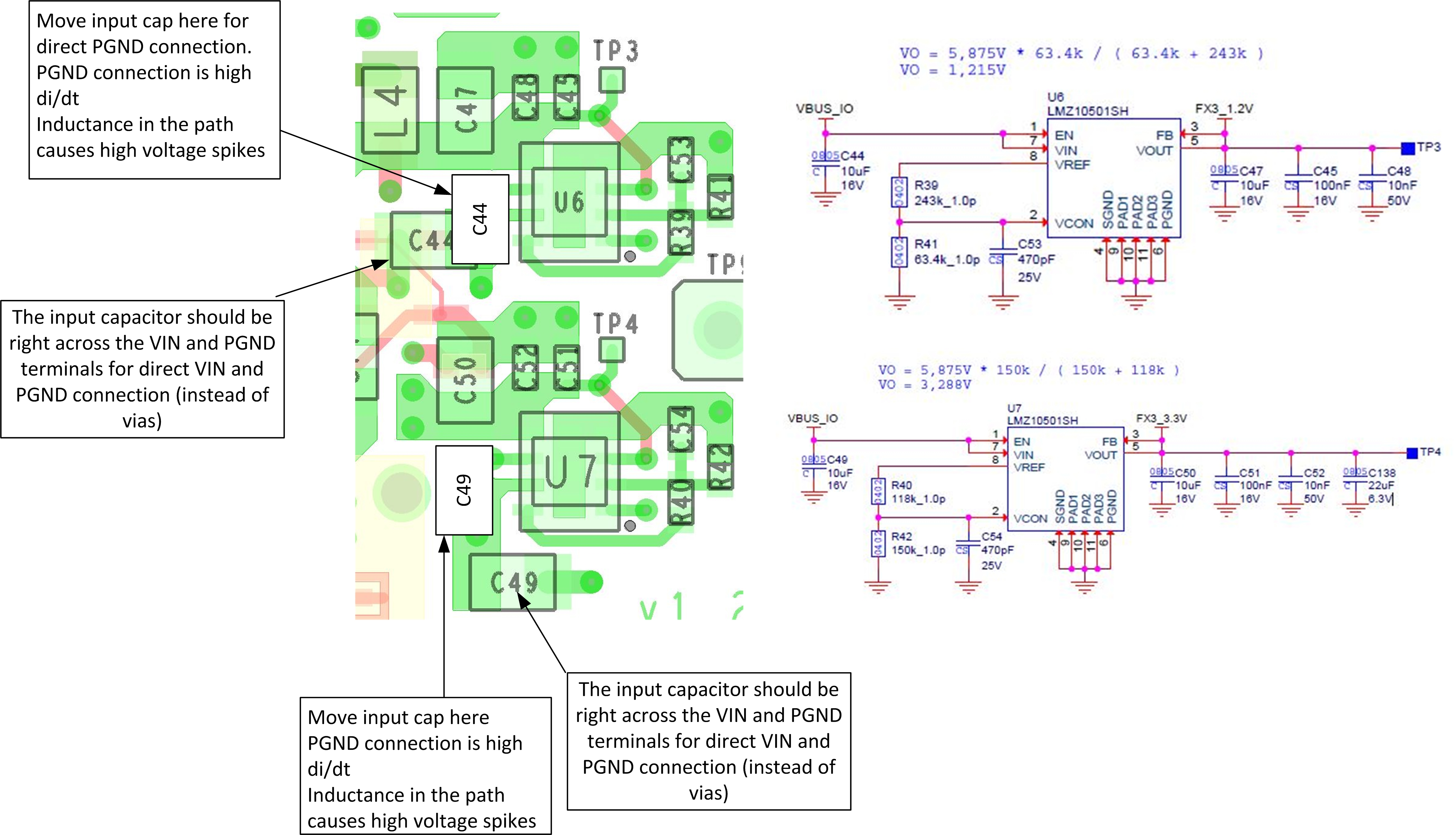
Could it be a false implementation of the device to the pcb? Maybe one of the 3 ground pas on the bottom has no connection anymore?

Best regard,

Marian

  • Hello Marian, 

    It seems that the enable circuit got damaged somehow. Is there a time when VIN is not up yet and EN voltage is being applied? The voltage on EN should always be less than or equal to VIN. Is the failure reproducible if you replace the device? Is there any visible physical damage to the device?

    The 3 pads on the bottom are not connected internally and should not make a difference.

    I will be happy to look at your schematic and layout if you would like. Please attach them here. 

    Regards, 

    Denislav

  • Here are my Schematic and Layout. As you can see copy & paste is a strong feature. I sticked to the layout recommended in the datasheet. Design 1 and Design2 are nearly the same. The only difference is the output voltage Design1 = 3.3V, Design2 = 1V.

    At the moment i investigate Design1. Another fact i could found out is that the resistance between input voltage (5V) and ground is 0 Ohm. So there should be a shortcut! But the only thing the 5V voltage is connected to is the LMZ10501. There is no other connection on the board, except a plug. Fortunately i am working for a thermography company so i can locate hotspots on the boards and even measure the temperature. And the only hotspot i can see is the LMZ10501. Sould there be a PCB failure the shortcut would be much higher than the 0.25A.

    Regaring your question:

    Is there a time when VIN is not up yet and EN voltage is being applied? --> That should not be happen because the pin is left floating. My test with the EN-pin was after the failure.

    Is the failure reproducible if you replace the device? --> That should take a while to next week because we cannot change the device.

    Is there any visible physical damage to the device? --> I do not see something suspicious. what should i look for?

    Best regards,

    Marian

    Untersuchung_LMZ10501.pdf
  • The input resistane went from 0 Ohm yesterday to 50 Ohm today. Wich result in the (exactly) 100mA higher power consumption as the working parts. 

  • Hi Marian, 

    I don't see anything suspicious with the layout. I think you did a good job of following the example layout in the datasheet. 

    What is the voltage rating of the input capacitor and is there any overshoot on the 5V input supply during startup? 

    If you are getting a short from VIN to GND, one suggestion is to try to solder reflow the IC pads just to eliminate the possibility of any solder smearing under the IC. Also, check the input capacitor terminals. It is probably unlikely scenario, but it is fairly easy to try this exercise. 

    In terms of physical damage to the part, it is also unlikely but take a look at the die on top of the device with a magnifying glass or bench microscope. Inspect the die for any structural damage at the corners that may have occurred during handling.

    Finally, if you can replace the device it would be valuable to see if this failure is consistent.

    Regards,

    Denislav

  • The good thing is we could finally solve the problem on all boards by replacing the LMZ10501 with a new one. The device is working fine again and no problems remain.

    The bad thing is that this problem could easly come again out of nowhere and remains undetected until the overheat protection disables the output voltage. So using the LMZ10501 can be a risk. We will have an eye on this and hope that these parts are the only ones.

    But to answer your questions:

    What is the voltage rating of the input capacitor and is there any overshoot on the 5V input supply during startup? 

    - The input capacitor is a GRM188R60J106ME47D with 6.3V

    - I tried the boards in system and with a labratory power supply with no difference. There sould not be any overshoot. The problem first occured by using a labratory power supply.

    If you are getting a short from VIN to GND, one suggestion is to try to solder reflow the IC pads just to eliminate the possibility of any solder smearing under the IC.

    - Unfortunately the ics were replaced without retrying the same part. But i doupt it that the connection between ic and pcb was the concern because the party were working for a couple of days/weeks without any issue. Also the amount 3/30 boards seems pretty high. I could not measure the shortcut from Vin to GND the next day.

     Also, check the input capacitor terminals.

    - No problems here either.

    In terms of physical damage to the part, it is also unlikely but take a look at the die on top of the device with a magnifying glass or bench microscope. Inspect the die for any structural damage at the corners that may have occurred during handling.

    - One part looked not with smearing on top but the other two were fine and looked like new.

    Could an ESD be the reason for this problem? Do you have heared of anything like that?

    Regards,

    Marian

  • Hi Marian, 

    If you kept the bad units, could you send those to us for analysis? 

    Regards, 

    Denislav

  • The good news is that i could get my hands on the replaced parts.

    The bad news is that one of the four devices was damaged by the process. The inductor on top of the LMZ10501 is gone. But you still got at least 2 parts. There are four because i killed one of the devices with my investigation due to a shortcut i guess. The device won't do anything.

    Could you please give my an address so i can send the devices?

    Regards,

    Marian

  • Marian, 

    Thank you for tracking those down. 

    You can ship it to:

    Texas Instruments

    Attn: Denislav Petkov

    2900 Semiconductor Dr

    Santa Clara, CA 95051

    USA

    Regards, 
    Denislav 

  • Soory but it is still an open topic.

    We have got some additional failures.

    Did you get my parts? Any update on them?

  • Hello Marian, 

    Unfortunately, I don't recall getting the parts but I will look through my archives again. It looks like this was more than 2 yrs ago. If you can, please save the new failed units in case we need to submit them for failure analysis.

    Is the failure you are getting the same as before ?

    Also, can you confirm which package you are currently using?

    The LMZ10501 package was updated recently (I believe in January this year). The new package has a different construction but it is pin to pin compatible version. 

    Here is a picture:

    The old "SH" device had an inductor on the bottom and a bare die mounted on top. The new construction (SIL package) has the inductor on top of a small PCB substrate. The die is embedded inside the PCB. This construction is more friendly in terms of device robustness during assembly (i.e. there is no exposed die to the outside world).

    Regards, 
    Denislav

  • Hello all,

    unfortunately we are facing quite a similar issue with these parts, lately.

    We are using both versions of LMZ10501 for some time in one of our designs to generate two power supply rails (1.2V and 3.3V) for an usb3.0 peripheral controller. Attached are some details about the schematic design and the layout. Lately, customers are reporting stability issues with these parts. During power on one of the parts might get very hot and fail. Thereafter various shorts from input and/or output voltages to GND are measureable. After some investigation the customers reported, that the parts may fail, when input power supply (VBUS_IO) is not derived from the usb line, but from an external 5.0V power supply unit. Is it a known issue, that the parts can get damaged due to some faulty input voltage? Voltage level is 5.0V and noise or spikes should not be the problem, but is there a limit for the rise time of the input voltage, for example?

    Best regards

    Michael

  • Hello Michael,

    Thank you for attaching the board layout. One thing I can point out is that the input capacitor placement should be improved. The PGND connection from the input capacitor GND to the device PGND pin is poor. It goes through a trace and via to another layer. This is a very high di/dt path (in a buck converter). If the input capacitor GND is not close to the device GND, the inductance in that path x the high di/dt will generate high switching voltage spikes every clock cycle. This could stress the device above its abs max rating, and is true for any buck converter.

    I am attaching a picture with my comments.

    Are you using the "LMZ10501SH" device or the "LMZ10501SIL" device?

    Parts can get damaged with a faulty input supply, if the supply voltage exceeds the abs max rating.

    Is the 5V supply well regulated, could it go above the 6V max operating?

    Does the failure occur during startup or after some time?

    Is the 5V supply ramp up very fast? Inductance between the supply and the input ceramic capacitors can ring up to higher voltage if the input is hot plugged or the input ramp is very fast. I would suggest using an oscilloscope to monitor the input voltage during startup to see if there are any transients above the abs max rating on the input of the device.

    Cheers, 

    Denislav

  • Hello Denislav,

    Thank You for the quick reply and the hint with the input capacitors. We will discuss doing a redesign, but up to now I am not totally convinced, that it is the admittedly bad placement of these what produces the problem we are facing.

    The boards we are talking about are being manufactured for about two years now. In the past we have been using "LMZ10501SH" devices and recently updated to the new "LMZ10501SIL". We are facing the issue with both revisions. The first reports arrived us only some weeks ago, when our customer changed the supply scheme of the boards (or better his adapter-boards) from "bus-powered" by USB to "self-powered" by an external 5V power supply unit. Not all devices are affected at once, but if they get damaged, this occurs right after power-on. So my guess would be, that something with the external supply is amiss. According to our customer the 5.0V supply is well regulated and respects all the maximum ratings. Unfortunately my request for specifications about the power supply unit in use, or even better, some pictures of the power supply ramp up have not been answered, yet. But I am at it.

    Please find some measurements attached, that I did with one of the boards. The pictures show some differences in the power-on behavior of the dc/dc converters when powered by USB ( 1.0m cable length) or by an external power supply unit, that ramps up quite slow. Using the very same unit, but connecting the board only after the 5.0V was already stable, results in plots comparable to the ones from the USB powering scheme.

    USB:


     External power supply unit:

    Yellow: Input supply for the dc/dc converters (5.0V); Blue: 1.2V output (U6); Green: 3.3V output (U7).

    Do I have to worry about the "step" of the 1.2V regulator? Is this, because the supply unit is not capable of sourcing enough current during power-on? Is there a maximum ramp up time for the power supply you would suggest to meet?

    Cheers,

    Michael

  • Hi,

    please find attached pictures sent by a customer showing power supply ramp up with their electronics. Blue = 5.0V input, purple = 3.3V output, yellow = 1.2V output. What do you think about these? Not really smooth, but no overshoot as well. Anything else, that I should worry about? Since my first post, no further parts were damaged...

    Best regards,

    Michael

  • Hi,

    any news for me?

    Replacing the damaged LMZ10501 on one of the damaged electronics, solved the issue there, the board is working again as expected. So it really looks like something is damaging the LMZ10501 during power-on. Our customer uses various power supply units to power their electronics. Is there a recommendation for the power-on behavior of a power supply unit used with the LMZ10501 besides maximum input voltage? For example minimum / maximum ramp-up time, minimum current drive capability during ramp-up? Any hints are welcome.

    Best regards,

    Michael