This thread has been locked.

If you have a related question, please click the "Ask a related question" button in the top right corner. The newly created question will be automatically linked to this question.

TPS65070 AC enabled

Other Parts Discussed in Thread: OMAP-L138, TPS65070, TPS65070EVM-430

Dear E2E:

Thank you for your help.

I use TPS65070 to power OMAP-L138. Everything looks good and works OK.

I use also embedded ADC converter for the different voltages measurement and this also works OK.

I have the question about possible accidental power shutdown by the SW through I2C0 interface.

1.  I use AC power (5V) input Pin10.

2.  In the DS page43 - Register PPATH1 bit[4] "AC power enable" can be set ='1' to disable AC power input.

3.  What is going to happen if SW accidently set PPATH1_bit[4]=1 (AC power input is disabled)? It is not clear from the data sheet but since AC input is the only one power source - all DCDC converter outputs will be shutdown. Is this correct?

4.  How the system can recover from this "shutdown"?

5.  AC input will still have +5V active and POWER_ON input is still high. Will TPS65070 restart again with default values? It is not clear from the data sheet.

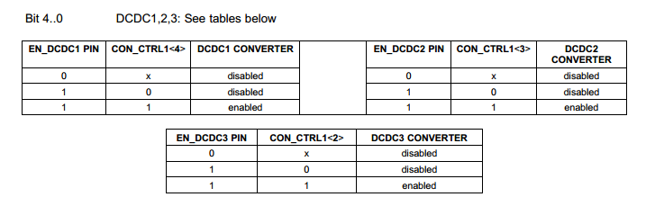
6.  In DS page53 - Con_CTRL1 register bit[4:2] for DCDC1:DCDC3. It is not exactly clear - now these enable bits function.

7.  DCDC2 and DCDC3 are automatically power-up sequencing. So the enable pins for DCDC2 and DCDC3 are tired to GND (page53). "The CON_CTRL1 Bits are automatically reset to default when the corresponding enable pin is low". How to understand that? Does it mean - the DCDC2 and DCDC3 will restart again after being disabled by writing '0' to bit[3:2]. Or according to the Tables on page54 - the state of bit[3:2] don't care?

8.  EN_DCDC1 pin controls the DCDC1 since [DCDC_SQ2:DCDC_SQ0] bits[7:5]=011. DCD1 is not the part of automatic sequencing. In this case CON_CTRL1_bit[4] can disable DCDC1. Is it correct?

9.  Will DCDC1 restart again after that automatically? What is required to restart the DCDC1?

Thank you very much for your help,

Boris Ruvinsky


  • Regarding, your first question, "what happens when AC is the only power source and is disabled through I2C by setting PPATH1[4] = 1?"

    SYS will begin to ramp down to UVLO at which point the converters/LDOs will shut off, the I2C registers will reset to their default values (including PPATH1) and the PMU will turn back on. 

    4024.D000.TIF

  • Hi Daniel.

    Thank you very much for your respond and explanation.

    Can you please answer also on my othe questions abour CON_CTRL1 register?

    6.  In DS page53 - CON_CTRL1 register bit[4:2] for DCDC1:DCDC3. It is not exactly clear - now these enable bits function.

    7.  DCDC2 and DCDC3 are automatically power-up sequencing. So the enable pins for DCDC2 and DCDC3 are tired to GND (page53). "The CON_CTRL1 Bits are automatically reset to default when the corresponding enable pin is low". How to understand that? Does it mean - the DCDC2 and DCDC3 will restart again after being disabled by writing '0' to bit[3:2]. Or according to the Tables on page54 - the state of bit[3:2] don't care?

    8.  EN_DCDC1 pin controls the DCDC1 since [DCDC_SQ2:DCDC_SQ0] bits[7:5]=011. DCD1 is not the part of automatic sequencing. In this case CON_CTRL1_bit[4] can disable DCDC1. Is it correct?

    9.  Will DCDC1 restart again after that automatically? What is required to restart the DCDC1?

    Thank you very much for your help,

    Boris Ruvinsky

  • In regard to your second question, "what happens to DCDC1 which is not part of the automatic sequencing for TPS65070 when the registers get reset to their default values?"

    If EN_DCDC1 is kept high, DCDC1 will turn on first (soon after SYS ramps up); this is the case unless  the external enable signal is driven low.
    The register CON_CTRL1 will reset to it's default values as well when SYS goes below UVLO. CON_CTRL1[4] is don't care if CON_CTRL[7:5]=011.

  • Hi Daniel.

    Thank you for you help.

    The scenarion for the questions 6:9 is a little different:

    1.  VSYS is stable - AC Power is enabled

    2.  SW accidently changed the state of CON_CTRL1_bit[4:2] to disable DCDC1, DCDC2, DCDC3. SW Set bit[4:2]='0".

    3.  DCDC2 and DCDC3 are automatically sequencing (CON_CTRL1_bit[7:5]=011) - so there "enable pins for the converters that are automatically enabled, should be tied to GND" (page53) .

    4.  "The CON_CTRL1 Bits are automatically reset to default when the corresponding enable pin is low" (page53). How to understand that? Does it mean - the DCDC2 and DCDC3 will restart again after being disabled by writing '0' to CON_CTRL1_bit[3:2]. Or according to the Tables on page54 - the state of bit[3:2] don't care?

    5.   EN_DCDC1 pin controls the DCDC1 since [DCDC_SQ2:DCDC_SQ0] bits[7:5]=011. DCD1 is not the part of automatic sequencing. In this case CON_CTRL1_bit[4] can disable DCDC1. Is it correct?

    6.  Will DCDC1 restart again after that automatically? What is required to restart the DCDC1 in case when VSYS is stable?

    7.  DCDC1 starts the last and DCDC3 starts the first according to TPS65070 DS, page73. Is it correct?

    Thank you very much for your help,

    Boris Ruvinsky

  • In your described scenario, DCDC1 will start first if you leave EN_DCDC1 high. 

  • Hi Daniel.

    Thank you for your help.

    1.  Can you please explain in more details?

    2.  If I understood correctly - DCDC1 will restart automatically after CON_CTRL1[4] set to '0' (DCDC1 disabled). Is it correct?

    3.  What about DCDC2 and DCDC3. Can they be disabled by SW - CON_CTRL1[3:2]=00? In DS page50: "The CON_CTRL1 Bits are automatically reset to

    default when the corresponding enable pin is low".

    4 Will DCDC3:DCDC2 restart immediately after the SW set CON_CTRL1[3:2]="00"? How long will it take to restart DCDC3:DCDC2?

    5.  Does it mean - SW can not disable DCDC3:DCDC2 which are the part automatic sequence? In DS: "The enable pins for the converters that are automatically enabled, should be tied to GND".

    6.  DCDC1 can start only after DCDC2 (1.8V) in my design - so it will start after 1.8v if 1.8V was disabled. Is it correct?

    7.  SW can create any erroneous combinations of CON_CTRL1[4:2].

    8.  The worst combination - if DCDC3 (1.2V) is disabled (CON_CTRL1[2]=0). That is because 1.2V must be ON first (the DCDC_SQ[2:0]=011). 

    Thank you for you help,


    Boris Ruvinsky


  • Hi Daniel.

    Thank you for your help.

    I would like to add one more question about CON_CTRL1 register

    The tables on DS page53 show that bits[4:2] are don't care (x) when EN_DCDC1:EN_DCDC3 are '0'. Is it correct?

    That means - the SW can't disable DCDC2:DCDC3 by setting CON_CTRL1[3:2]="00" because pins EN_DCDC2:EN_DCDC3="00" (the SQ2:SQ0="011" for OMAP-L138). Is this true?

    Thank you very much for your help,

    Boris Ruvinsky.

  • Have you looked into getting an EVM to evaluate the IC? TPS65070EVM-430

  • Hi Daniel.

    Thank you for your respond.

    I think - this kind of information must be clear from the device DS.

    It is a pure question about the device TPS65070 logical behavior.

    Can you please find from the factory engineers - how the device TPS65070 should behave in case if SW is trying to shutdown DCDC3 and/or DCDC2 through the CON_CTRL1 register[B3:B2] when DCDC3 and DCDC2 are the part of the automatic sequencing (DCD_SQ2:DCDC_SQ0= 011)?

    Thank you,

    Boris Ruvinsky

  • Boris, will you please provide the volume and application for the TPS65070?

    Per testing in the lab on an EVM, the following tables only apply if the converters are set to enable by the external pins. 

    So in your example where CON_CTRL1[7:5] = 011, DCDC2 and DCDC3 can be enabled/disabled using CON_CTRL1[3:2] even if pins EN_DCDC2 and EN_DCDC3 are tied low; in this example, pin EN_DCDC1 would have to be tied high in order for the software to enable/disable using CON_CTRL[4].

    If you are changing CON_CTRL1[7:5] on the fly, in some cases the new power-up sequence must be triggered, e.g. POWER_ON pulled low, then PB_IN pulled low and POWER_ON pulled high then PB_IN released.

  • Hi Daniel.

    Thank you for your help.

    I wan to answer to your question:

    1.  We are developing in Goodrich the avionics products mainly for the military.

    2.  Our volume is not very big - it is in the range 1000-5000/year

    3.  But the life of the product is long - it is in the range of 10-20 years

    And one question on the TPS65070 DS:

    How should I understand these words from DS?

    "The following tables indicate how the
    enable pins and the CON_CTRL1 register are combined. The CON_CTRL1 Bits are automatically reset to
    default when the corresponding enable pin is low".

    Does it mean - the DCDC3 and DCDC2 will recover because "The CON_CTRL1 Bits are automatically reset to
    default when the corresponding enable pin is low"?
    Is it true?

    Thank you very much for your help,

    Boris Ruvinsky