This thread has been locked.

If you have a related question, please click the "Ask a related question" button in the top right corner. The newly created question will be automatically linked to this question.

TPS23754 with 24V output

Other Parts Discussed in Thread: TPS23754, TPS23753, TPS23754EVM-420

I am working for a VoIP project, the design of the basic functions is close to be finished but I have not designed the PoE part yet. I have not much knowledge on the PoE and DC/DC power supply, as I am better on "software and digital things"....I found the TPS23754 may be good for my product and I can found an application guide "PoE Powered Device for 24Vac Building Power Applications" ( SLUA477 ) http://www.ti.com/lit/an/slua477/slua477.pdf . This application is good because it shows how to implement the PoE and an additional Aux Input, that is what I need. However, my product need a 24Vdc output, rather than the 12Vdc output in this guide. I know the transformer need to change to 24V secondary, but what else is needed?

Could you advise how to modify the circuit (or advise another circuit) so that I will have a 24Vdc output?

Thank you very much

  • Thank you, could you advise why the TPS23754 need the second gate drvie output (GAT2) but the TPS23753 do not need it? The TPS23753 reference desgin seems much easier.

  • IEEE802.3at provided for twice the power of IEEE802.3-2005.  Customers became more concerned with efficiency. 

    The second gate driver provides native support for designers to make cost/efficiency/complexity tradeoffs using more sophisticated topologies.

  • According to the answer, so we can connect the gate of MOSFET Q1 directly to the "GAT2" pin, and remove the T3, Q3, D17, C27, R23 and C28?

    However, if we need solution with isolation, then the T3 part can not be removed, is it correct? 

  • Much more information is required to provide an accurate answer. Please write up a detailed specification of your system requirements (output conditions, input conditions including adapter and POE sources, safety, isolation, cost, efficiency, etc.) and we can point you to an internal reference design which may suit your needs.

  • I took reference to the TPS23754EVM-420 and built a test board, but it is not working, please check the attached schematic of my testing board. Could you help to check what is the problem?

    The PoE should be able to connect with both 802.3af and 802.3at PoE source (when conect to 802.3af the output power requirement is lower). Output is 24Vdc +/-5%, efficiency higher than 80%, need isolation. The Aux input is 24Vac. The cost around USD4.5.

    I have bought some TPS23754 and made the BOM, so I hope to keep using this IC.

    Sorry for my late reply because the project is lagged by something else, but please reply  asap because the project started again and have to be finished urgently.

    Thank you very much

    5432.AF12-PB(25W)(Testboard)-rev0.pdf

  • I cannot find the primary side switching MOSFET in your schematic (refer to Q2 in HPA420 or TPS23754EVM-420). Also, the VOUT setpoint resistors do not seem to be chosen properly for a 24V output (R19, R13). FYI, the schematic is mirrored in the PDF so is hard to read).

  • I am sorry for the mirrored pdf.

    I have just able to received the MOSFET and the related resistors, I built a test board again for testing the power supply, but I still can not get a 24VDC at the output. The circuit is still reference to the TPS23754DVM-420 and changed the circuit according to: http://e2e.ti.com/support/power_management/power_interface/f/204/p/129664/690037.aspx#690037

    I have attached the modified schematics here.

    5857.AF12-PB(Test1).pdf

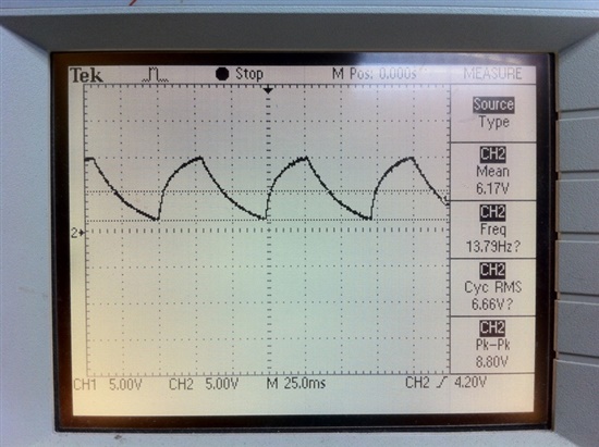
    At the moment I have just tested the external input. If there is no load, the output voltage will vary (around 23~27V depends on the input voltage). If I use a 420R resistor for the load, the output will drop and a typical capacitor charge and discharge waveform can be observed, please refer to the attached screen capture of the output.

    Basically I require a PoE PD device with external 24Vac input as well. The output is 24Vdc, 20W.


  • Your new schematic is much better and seems to match the modify instructions given earlier for the TI TPS23754EVM-420 for 24V output.. TI built and validated those instructions with lab testing so we are confident the circuit is fine. Maybe there is an incorrect resistor value or connection on your test board?

    The waveform above can occur because the TPS23754 converter is cycling. This will occur by design in an output overload condition and is referred to as "hiccup". This can also occur when there is an issue with the auxiliary bias voltage (at the Vc pin). Check R201, D202 circuits and measure that voltage with a) no load and b) loaded as above. THis dc voltage should be at ~12V under normal circumstances (below 9V will shut off the converter and converter will restart when Vc is above 15V (~6V hysteresis).

    I would also suggest using several ceramic capacitors on the output (at C205 location). I suggest 3x 10uF 50V ceramics.

  • Eric, you are right, I found that the TPS23754 and the Vc pin are cycling. I found that it is because the soldering pads of the optocoupler on the PCB were swapped. After I fixed it, the output is at 24V for no load or very small load (below 100mA). However, the ripple output voltage is high (around 1.5V). Also when I increase the load to about 100mA, the voltage drop significantly.

    Also, I would like to ask what is the function of D203, C204 and R202 at the secondary of the transformer? I am wondering if this part is correct because it is not at the TPS237540-EVM reference design and I modified it as I didn't use the gate2.

    Thank you very much.

  • Also when I increase the load to about 100mA, the voltage drop significantly. Verify your circuit connections again. The TI 24V output circuit was tested and proven to work.

    What is the function of D203, C204 and R202 at the secondary of the transformer? D203 is the output rectifier (the TI EVM with 5V output uses a synchronous rectifier instead of a diode rectifier and therefore needed GAT2). C204/R202 is a voltage snubber to reduce switch node ringing.