This thread has been locked.

If you have a related question, please click the "Ask a related question" button in the top right corner. The newly created question will be automatically linked to this question.

Design Check

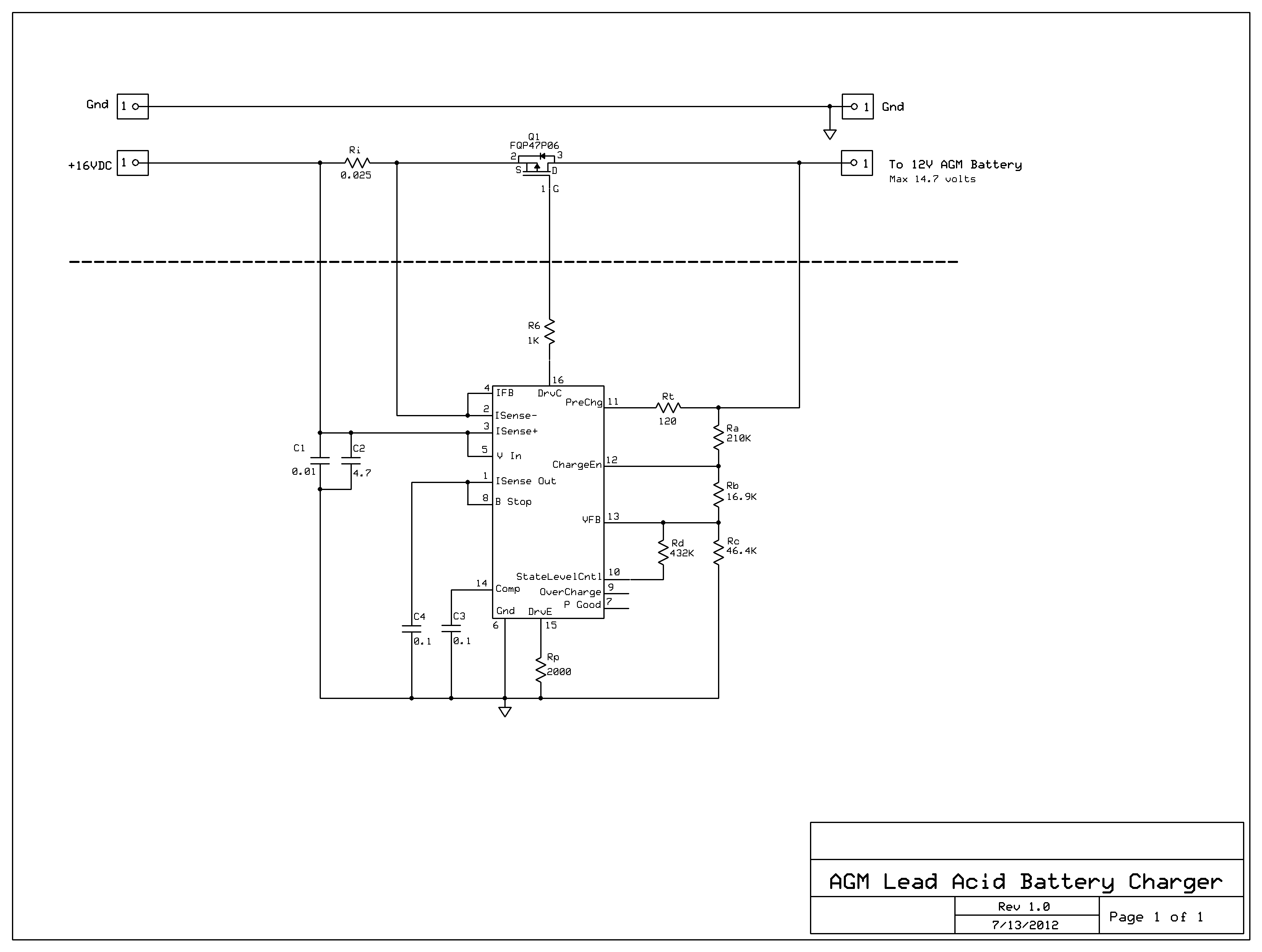
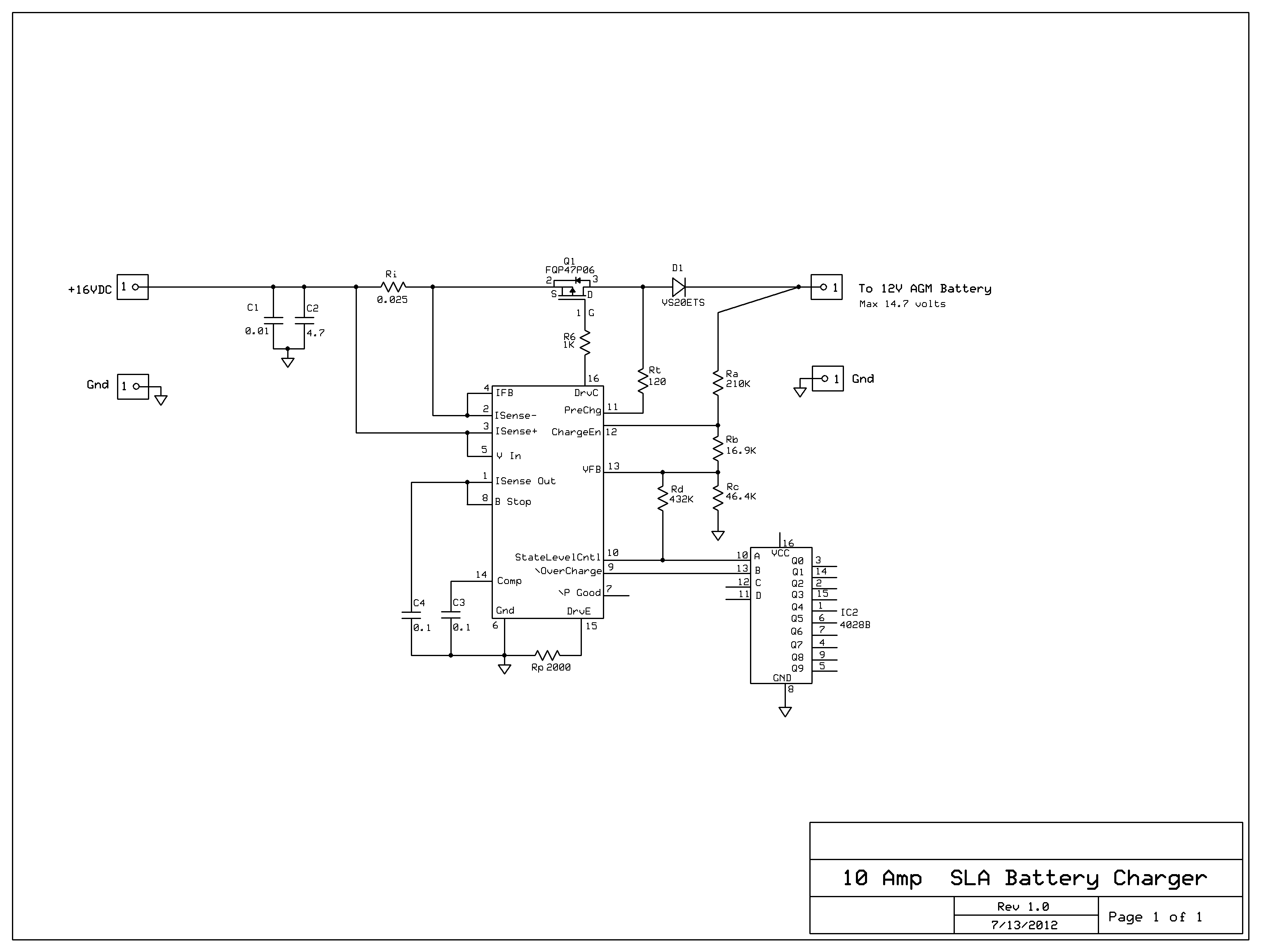
I wonder if you could comment on my design for a 10 amp charger for a 12 volt SLA battery.  It will be AC powered with a DC input of 16 volts when the AC is 115 VAC.

Other design parameters are fast charge at 14.7 volts, float at 13.5 volts, and final discharge of 10.5 volts.

I am also interested in any comments on my selection of the FQP47P06 as a pass element.

Also do I really need D1 since the battery is over 100AH, the discharge thru the circuitry is trivial?

I am also not sure about the values for Rt and Rp.  I calculated the value for Rp from the evaluation module notes.

I calculated Rt based on:  It = Vin - Vt - Vdrop/Rt,  where It = .025 amps.

  • I guess I don't understand how this forum works.

    I thought someone from TI occasionally perused the forum and responded to questions.

    Did I post in the wrong area or something?

    Pat

  • It is best to contact the local Field Rep.

  • Apparently TI is not interested in helping.

    Anyone else have any comments?

    The nature of the subject makes it somewhat difficult to verify a design without possible damage to an expensive battery, so any and all comments will be appreciated.

    Pertinent parameters of the FQP47P06 are:

    60V P-Channel MOSFET

    Absolute Maximum Ratings TC = 25°C unless otherwise noted
    Drain-Source Voltage -60 V
    Drain Current - Continuous (TC = 25°C) -47 A   - Continuous (TC = 100°C) -33.2 A
    Drain Current - Pulsed  -188 A
    Gate-Source Voltage ± 25 V
    Single Pulsed Avalanche Energy 820 mJ
    Avalanche Current (Note 1) -47 A
    Repetitive Avalanche Energy (Note 1) 16 mJ
    Peak Diode Recovery dv/dt (Note 3) -7.0 V/ns
    PD Power Dissipation (TC = 25°C) 160 W   - Derate above 25°C 1.06 W/°C

    Off Characteristics
    Drain-Source Breakdown Voltage VGS = 0 V, ID = -250 μA -60 -- -- V
    Zero Gate Voltage Drain Current   VDS = -60 V, VGS = 0 V -- -- -1 μA    VDS = -48 V, TC = 150°C -- -- -10 μA

    On Characteristics
    Gate Threshold Voltage VDS = VGS, ID = -250 μA -2.0 -- -4.0 V
    Static Drain-Source On-Resistance VGS = -10 V, ID = -23.5 A -- 0.021 0.026 Ω
    Forward Transconductance VDS = -30 V, ID = -23.5 A -- 21 -- S

  • The following is the response from TI support:


    Thank you for your interest in Texas Instruments products and services.  We value your technical support request with Texas Instruments.

    Due to the nature of your inquiry, we recommend you use our TI E2E™ Community Support Forums where you can post questions, search for answers and collaborate with fellow engineers and TI experts.

    You can access the E2E forums through the following link: http://e2e.ti.com

    We appreciate your understanding and look forward to working with you in the future. We are continually improving our online community.

  • Pat,

    Did you ever get your issue resolved?  I am trying to design a charger using a PFET and there is not very good information out there.  In looking at your design I have the following questions:

    How did you calculate a value for Rp?

    Do you not need a Dext because of the diode in the PFET?

    Does the PFET shut off properly or did you need to add a resistor between the Gate and Source?

    Thanks,

    Mike.