This thread has been locked.

If you have a related question, please click the "Ask a related question" button in the top right corner. The newly created question will be automatically linked to this question.

TPS61030 Bode Plot question

Other Parts Discussed in Thread: TPS61030

 Hi experts,

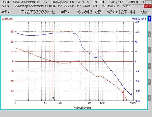
Customer design TPS61030 and Vin=4.6V; Vout=5V. And they measure Bode-plot in below picture.

Can you advice is there any concern if there is multi-crossover points when Gain is in 0dB?

Can you aslo advice what reason to cause these multi- crossover points?

Thanks

  • There are a few assumptions made when taking a bode plot.  The first is that the circuit is fairly stable--i.e. there is minimal jitter on the SW node.

    Another is that the circuit is operating in PWM mode, not power save mode.  Additionally, the IC should not be operating with either the minimum on time (low duty cycle) or minimum off time (high duty cycle), as these are large signal effects that corrupt the small signal bode response.

    Lastly, for this IC, they need to be sure and use the recommended output cap configuration of a small ceramic placed near the device followed by a larger capacitor with ESR.  Large amounts of ceramic capacitance downstream can cause instability.