


Hello,
I believe that the datasheet for the TPS40210-Q1 Boost controller contains an error in the formula for calculating the critical output current. The datasheet defines the critical current as the boundary between discontinuous conduction mode (DCM) and continuous conduction mode (CCM). This happens at the point where the inductor current falls exactly to 0 before the start of the next switch turn-on cycle. Figure 1 below illustrates this condition.
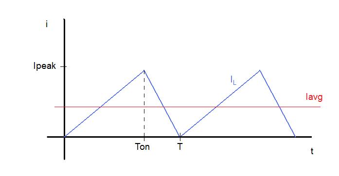
Figure 1. Inductor Current Boundary-Conduction Mode (BCM)
In a boost converter, the peak inductor current is given by:
(1) Ipeak = (Vin_max*Ton) / L
where Vin_max*** is the maximum DC supply voltage and L is the inductance value, and Ton is the on-time of the MOSFET switch.
Now since an inductor has minimal DC resistance it cannot sustain a DC voltage across it. Therefore the on-time Volt-Second product has to equal the off-time Volt-Second product. Thus:
(2) Vin_max*Ton = Tr * (Vout + Vdiode - Vin_max) and
(3) Ton + Tr = T = 1/Fsw for BCM
where Vin_max and Ton are the same as before, Tr is the off-time of the MOSFET switch, Fsw is the switching frequency, Vout is the desired converter output voltage, and Vdiode is the forward voltage drop of the freewheel catch diode.
Combining (2) and (3) and solving for Ton yields
(4) Ton = (T * (Vout + Vdiode - Vin_max)) / (Vout + Vdiode)
Substituting (4) back into (1) gives:
(5) Ipeak = (Vin_max * T * (Vout + Vdiode - Vin_max)) / (L * (Vout + Vdiode))
Now since the average inductor current must equal the DC load current, it follows then that the average inductor current at the onset of Boundary Conduction Mode (BCM) is the critical current for the converter. Any increase in load current will raise the inductor current minimum values to something other than zero to give the characteristic "Ramp-On-Step" wave shape of a continuous current mode inductor. Likewise any further decrease in load current from the average BCM current will result in the addition of dead time between the point where the inductor current reaches zero and the start of the next switching cycle. This is due to the fact that the slope of the inductor current remains constant as the value of L remains constant. This addition of dead time results in discontinuous conduction mode operation. So to find the load current where this transition occurs we find the average value for one cycle of the waveform shown in figure 1.
(6) Iavg = (1/2*Ton*Ipeak + 1/2*Tr*Ipeak) / T which reduces to
(7) Iavg = Ipeak / 2
Plugging (5) into (7) yields
(8) Iavg_critical = (Vin_max * (Vout + Vdiode - Vin_max) ) / (2 * L * (Vout + Vdiode) * Fsw)
For loads higher than the value calculated using (8) you will always be in CCM. For load values below that calculated in (8), you will be in DCM. However, this equation does not agree with the one published in the datasheet. The datasheet gives the critical output current as:
(DS4) Iout(crit) = (Vout + Vdiode - Vin_max) * (Vin_max)^2 / (2 * L * (Vout + Vdiode)^2 * Fsw)
The datasheet formula is identical to mine with the exception that the result is reduced by a factor of (Vin_max) / (Vout + Vdiode). (remember a boost converter always has Vout > Vin_max so that multiplier is always less than 1) According to (DS4), a CCM boost converter stays in CCM at a much lower Iout than I would predict and conversely, a DCM boost converter switches to CCM much lower than I would have predicted as well. Can someone please explain why the critical (boundary) current would be less than the result given by (8) above?
Regards,
Shawn
***If you are wanting to find the maximum load current that can be drawn and still remain in DCM, replace Vin_max with Vin_min, or the minimum DC supply voltage the converter will see.


