Hello,
I'm interested in using the LMZ10501 nano-module in a high-reliability application.
Since the nano-module has a bare die that is mounted on top of an inductor with no underfill, I have a few concerns:
1) What happens to the exposed die after a long time in a humid environment?
2) Can dust particles or other contaminants that accumulate on the die over time cause any damage?
3) Are there any concerns when placing the device on a PCB? Are the standard SMT placing tools & methods suitable for the nano-module?
4) There seems to be some kind of a protective layer on top of the die. What is this layer? Was its long-time reliability tested?
5) After assembling PCBs, the boards are usually washed. Were the effects of PCB cleaning chemicals on the exposed die tested?
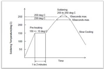
6) The nano-module is soldered to the PCB by a reflow process. That means that the die on top of the module is "double-reflowed". Can't this second reflow weaken the connection of the die to the inductor? Are there any special reflow procedures for the module?
7) What is the composition of the solder bumps on the die? If they are lead-free, is there a tin-whisker problem?
8) Is it recommended to protect the die by applying some kind of an encapsulation on it? Were there any tests done to understand the effect of an encapsulation on the device? If so what is the recommended protection for the device?
9) Was the module tested for mechanical shocks before and after soldering to a PCB?
If there are any reliability test data available that can be shared, I'd appreciate it.
Thank you,
David