This thread has been locked.

If you have a related question, please click the "Ask a related question" button in the top right corner. The newly created question will be automatically linked to this question.

lm5050-1 problem

Other Parts Discussed in Thread: LM5050-1

Hello,

we have a huge problem with lm5050-1 device. Everything is connected as in datasheet:

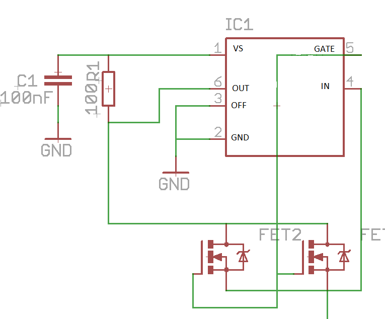
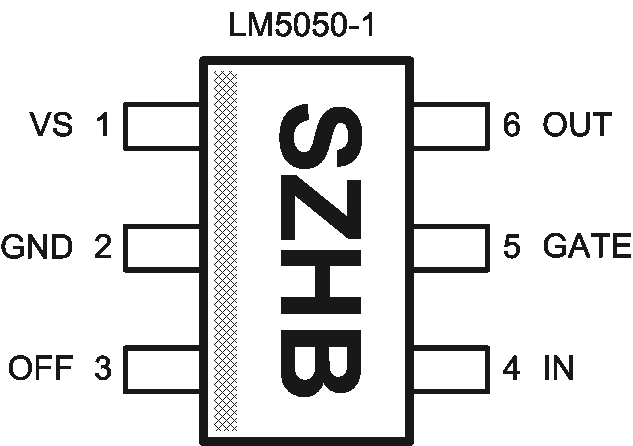
Pin1: via 100Ohm to mosfet-Drain, 100nF to gnd
Pin2: GND
Pin3: GND (always on)
Pin4: connected to mosfet source
Pin5: connected to mosfet gate
Pin6: connected to mosfet drain

We have two supply lines (+5V, +12V).

On +5V lm5050-1 drives gate voltage of mosfet to only 6.5V (this is hardly enough to be in conduction state)
On +12V lm5050-1 drives gate voltage to only 11.5V! Current flows through body diode, huge losses.


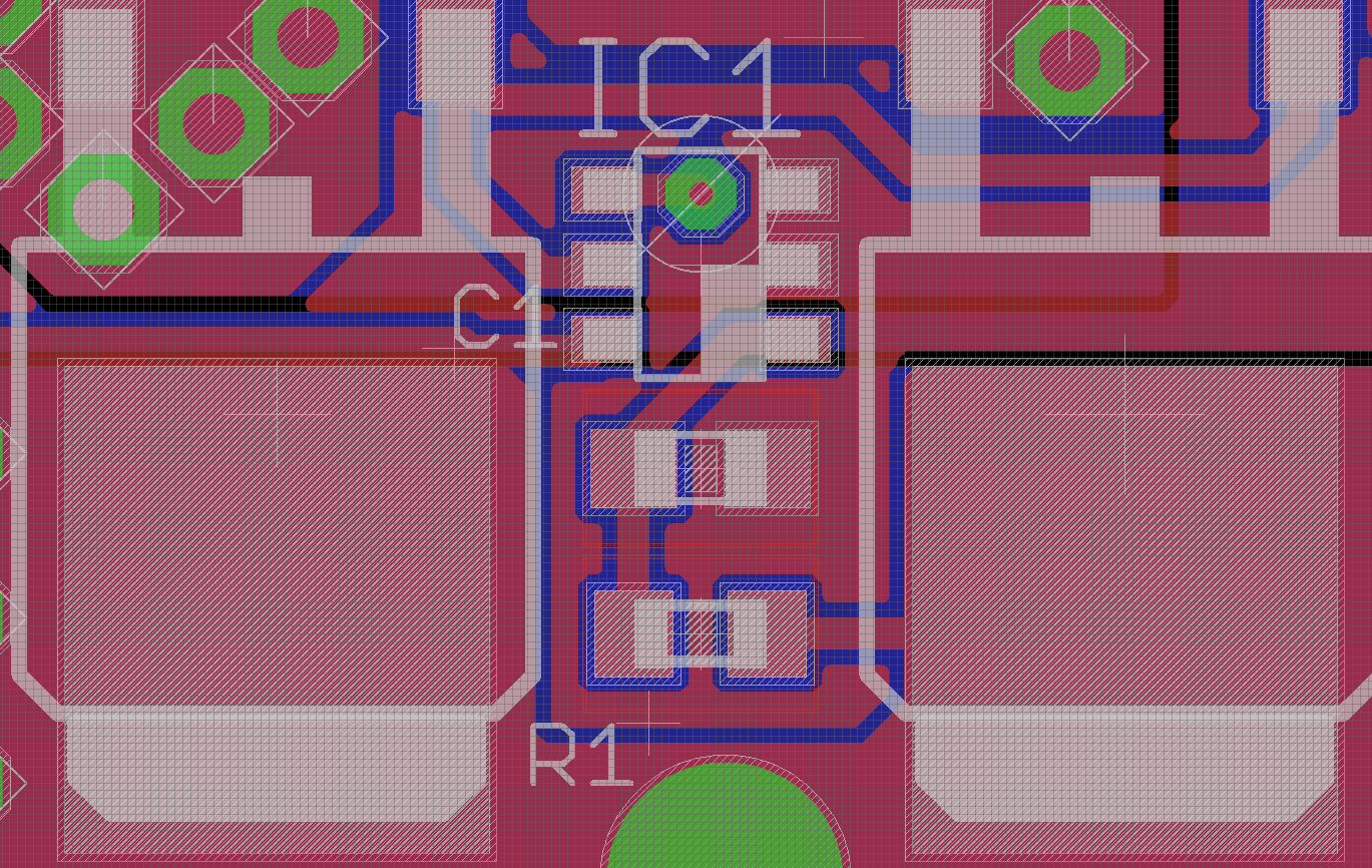
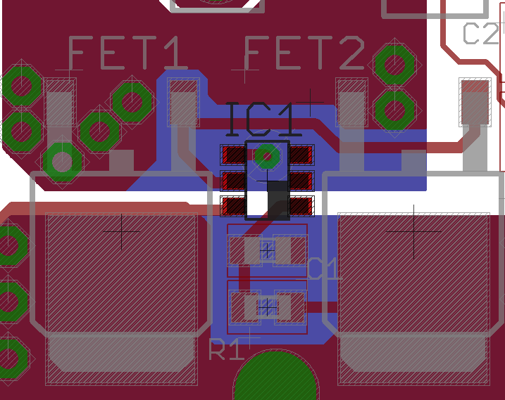
I have included a pcb picture. everything is shown except gnd connection.
c1 is 100nF, r1 is 100 ohm.


 What would you do to solve this issue?

Thanks! 

  • short clarification:

    This picture shows 2 parallel mosfets (+12V supply line).

    The same problem applys on our single mosfet +5V supply line.

    Thanks! 

  • Gnd connection to LM5050-1 pins 2 and 3 are not obvious in the pcb picture. Beyond those two pins I don't see anything that looks wrong.

    I presume the gate voltages you mention are with respect to ground.

    A schematic might be helpful, and part # for the mosfet.


  • Hello,

    the gnd connections are created by gnd polygon plane and visible in the following picture:


    Part number of mosfet:

    digikey: IRLR8743TRPBFCT-ND
    Mosfet N-Channel 30V 160A

    http://www.irf.com/product-info/datasheets/data/irlr8743pbf.pdf


    And schematic:


    We have 15 of this chips soldered (2 Mosfet in parallel for 12V operation, 1 Mosfet for +5V bus)
    All show same behaviour. Thanks for your help, we planned to do an initial run of several hundred  boards and didn't expect problems with this chip...

    Tom 

  • just to make sure:

    When I am reading "SZHB" on the device, the pin on the left bottom is pin 1, right?

    At moment there is no solution for this problem :(
    Is there anyone here using this chip?

  • " ... the pin on the left bottom is pin 1, right? ..."

    Yes, in addition there is typically a 'hard-to-see' impression in the package epoxy along the pin 1-2-3 side

    As for why this is not working ... I don't know. All the info provided says this should work


  • After looking at the data sheet this device may operate in a misleading fashion if there is a low output load current or if you have chosen a FET or FETs that are too low in RDS for proper function.  The device does reduce VGS until there is a constant ~25mV between Source and Drain - this may be why you are  seeing a lower VGS than expected.   If still in doubt I would remove the mosfet / mosfets from a PCB and then using a high impedance DVM (digital volt meter) check that the gate drive pin (pin 5) of the IC is higher by somewhere between 7 & 14 volts than the in or source pin (pin4).  Without mosfets fitted, you should find ~7V higher (ie 12V relative to gnd) with 5V applied, and ~14 volts higher (ie26V relative to gnd) with 12V applied).  This should tell you whether the IC is functioning.  Then test the FET ( put the DVM on diode test, apply + lead to the FET gate & - to the source.  Now being careful not to touch the Gate check the + to Drain and - to Source is low impedance - whilst doing this touch the gate/source with your finger & voila - high impedance again - if this occurs your FET is OK, you just charged the gate up with the diode test voltage, proved it could hold gate charge for a few seconds (usually minutes) and that the fet  turned on with the small Gate charge, and then off when the charge was removed .   Do use a CRO to check each pin of the IC (relative to ground) if you are still not making progress - you could find ripple or glitches or something else unexpected.  Dont give up - everything has an answer / reason - you just need to find it !  Perhaps noise (ripple) from the circuit at the output, is falsely triggering the reverse current comparator, in which case try increasing C1 or decoupling the output with an appropriate filter (capacitor ?) Good Luck !