This thread has been locked.

If you have a related question, please click the "Ask a related question" button in the top right corner. The newly created question will be automatically linked to this question.

TPS40055 shoot through

Other Parts Discussed in Thread: TPS40055, TPS40054


We have couple of DC/DC converters on our board based on TPS40055.   28V to 3.3 (3A)etc...  This one has a switching frequency of 683KHz.
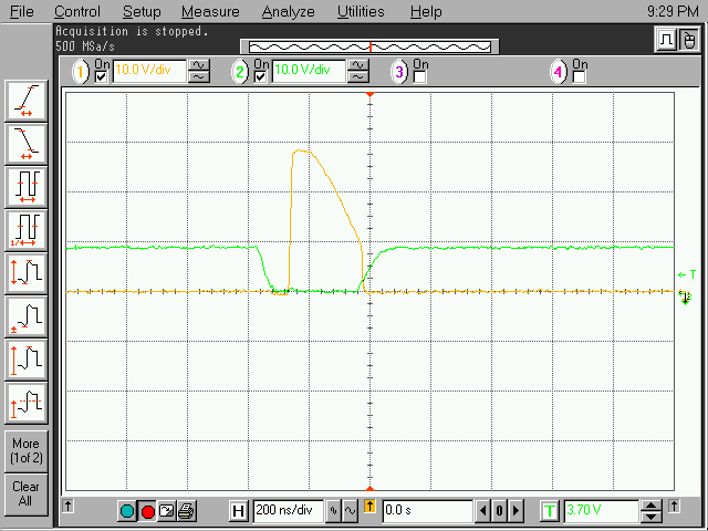
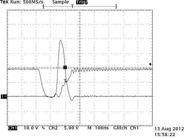
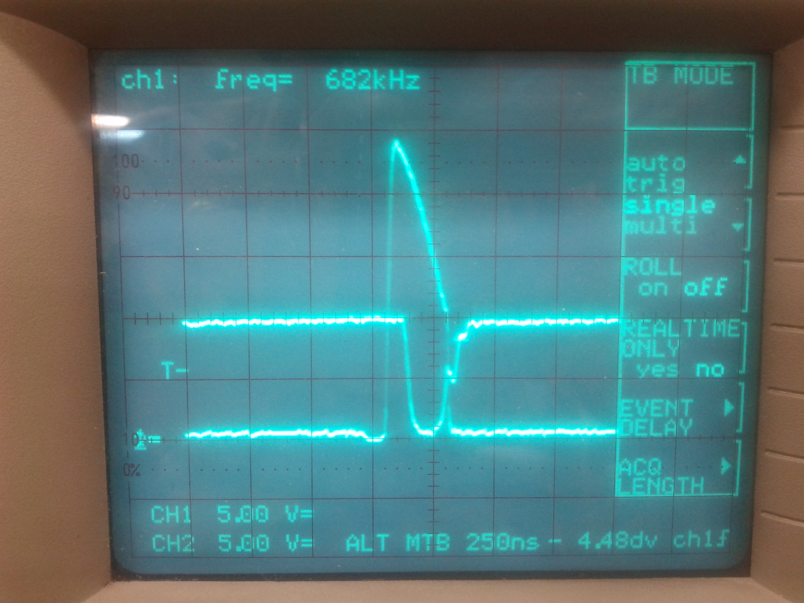
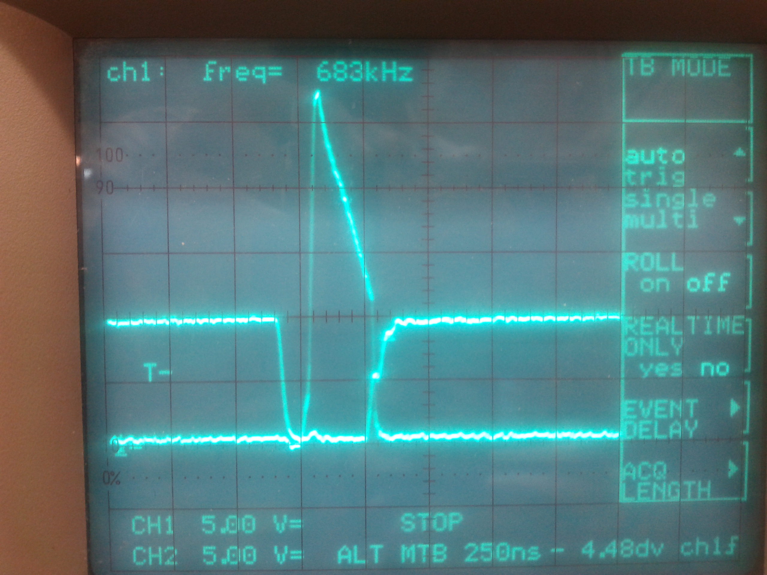
We are seeing that some of the rails are showing a very low (or none) delay between the SR fet turn On  and Primary switch turn off. Please see the attached waveforms: (the smaller trace is the Vgs of the SR fet and the other trace is the voltage at the switch node)
The gate voltage of the Primary fet is very similar to the switch node voltage ( 5 to 7 volts higher amplitude)
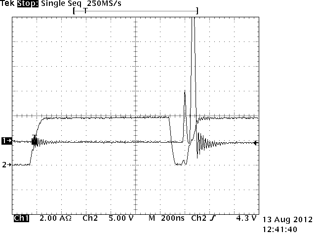
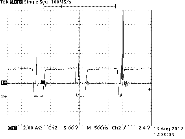
 Most of the time, the waveform looks like the second waveform, but occasionally the shoot through is observed as seen in firstwaveform. Although the circuit seem to work without too much heat dissipation in the current revision of boards, changing the Mosfets (to one with lesser gate charge Qgs )  makes the problem worse.

Currently we use the Vishay part  SI4470EY (obsolete now). We tried using the parts si4840bd and si4124dy and the problem gets worse

SI4470EY  and si4840bd are listed in the switcher pro database for this design. 1.Is it possible to adjust the turn on times of the SR fet in this chip. How? 2.Looks like the turn off the primary switch is very slow compared to turn On , Is this normal?

 After going through the support forum , I checked the volatges at all the pins of the controller and they are normal. Please provide suggestions to solve the shoot thoough problem.


 Thank you

Ashok

sync_buck_3v31.pdf
  • Hi ,

    I should add that this problem is seen in low load conditions. 

    Ashok

  • Hi Ashok,

    Are you questioning the time when SR fet turns on or the time when SR fet turns off? The first figure looks weird to me when the SR fet turns off. The SW node waveform has a deadtime before SW goes up high, but the Vgs of SR fet is still on. That makes me wonder how the Vgs of SR fet is measured. I don't think it is a real shoot-through, otherwise, the fets should already get burnt and SW node should not go straight up to Vin while the SR fet is still on. Another thing looks abnormal is the voltage drop on SW node waveform when the high-side fet is on. The Rds,on of the fet is only 10mohm, but the voltage drop is about 15V during on-time, i.e. 150A, which does not make sense. I would suspect there is huge resistance in series with the high-side fet.

    Regards,

    Na


  • Hello Na,

    Thankyou for the reply,

    I am more worried about the SR fet turn ONs , the turn off was a random event I captured . As you can see from the schematic, there is no resistor in series with the high side fet. Please note that the problem is seen in low load condition . At higher loads the waveforms looks fine as shown in second figure below.

    At lower loads , due to the shoot through the power supply draws too much current from the 28V and the FET will burn if I don't current limit the input 28V. At a higher load the current consumption reduces to normal and no shoot through is observed.

    Now I have some captures with a better oscilloscope.

    Green : SR fet gate, Yellow: Switch node voltage

    During 10% of designed load

    Higher load (say 40% of designed value)

    Thanks

    Ashok

  • Hi Ashok,

    The new waveforms are not shoot-through to me. Once the SW node starts to fall off, the high-side FET should be already off. Can you capture HDRV and LDRV together to help us get a better idea?

    Regards,

    Na

  • Thank you Na,

    Now I have captured the current consumption on 28V , which clearly show that both fets are conducting simultaneously. 

    Fig1: Both gates measured w.r.t gnd when the current spikes (smaller waveform is the SR gate)

    Fig 2: Current on 28V and SR gate voltage

    Fig 3: Every few cycles a shoot through is observed. ( Last time I missed the shoot through case)

    Note that the SR OFF pulse width is very low during failures

    ->Why does the SR OFF pulse width drastically reduces for some pulse . Is this normal. 

    -> How is the TPS 40055 supposed to behave in low loads?

    ->Is it ok to use TPS40055 at 10% of the designed load?

    Ashok

  • Hi Ashok,

    Thanks for the update!

    I agree with you that there is shoot-through happening for some pulses. It is possibly related to minimum on-time. For test purpose, can you try to lower down the input voltage or the switching frequency to see whether it helps?

    Regards,

    Nao

  • Thank You Na for the suggestion.

    I tried to reduce the switching frequency to 458khz and found that the shoot through is not observed even at low loads.

    However, we would like to operate at 600+ Khz. We would like to understand the behaviour of the controller at low loads.  Please let us know your thougts

    ->Why does the SR OFF pulse width drastically reduces for some pulse . Is this normal. 

    -> How is the TPS 40055 supposed to behave in low loads?

    ->Is it ok to use TPS40055 at 10% of the designed load?

    Also, We would like to explore the possibility of using TPS40054 which has the capability of going to non-synchronous buck mode at light loads. What is your opinion on that?

    Ashok

  • Hi Ashok,

    The TPS40055 should be working fine at low loads and even no load. This shoot-through is something abnormal.

    The input capacitance seems bit low. Have you checked the input voltage ripple? That could be a possible cause of the high-side drive short pulse.

    Another possibility is the high-side pulse is falsely terminated due to pulse-by-pulse current limiting. ILIM resistor should be connected to the drain of high-side FET instead of the quieter VIN of the controller IC. The controller compares the ILIM and SW voltage when high-side FET is on. As high-side FET turns on, there will be some voltage ringing on SW, as well as the drain of high-side FET. If ILIM is connected to a quieter VIN, the ringing on SW, especially the voltage dip, may be interpreted as an over-current condition to terminate high-side FET. But if that is the case, the high-side FET should be at least longer than the propagation delay of ~300ns. So I have not convinced myself that this is the cause of the short pulse. My point is the ILIM resistor connnection can be improved.

    You can use TPS40054. Special care needs to be taken for the loop design, which needs to work for both DCM at light load and CCM at heavy load. Another concern is the zero-current crossing detection circuit. The threshold can be -10mV minimum. Considering the 10mohm Rds,on of the low-side FET, the threshold is not quite accurate.

    Regards,

    Na


  • Hi Na,

    Thank You for the reply.

    I have checked the ripple, its is quiet good , less than 5%.

    On my board I have already shorted the inductor that is filtering Vin , so ILIM is connected to same node as drain of high side FET.

    I have another question:

    Is the 300 ns minimum pulse width a requirement for the controller to work normally. Can it cause shoot through if the pulse width is say 150ns

    I see that in the example given in the datasheet 400ns +10% margin is taken as the minimum . is this essential for the current limit to work?

    Thanks

    Ashok

  • Hi Ashok,

    If the pulse width is 150ns, comparable to the minimum controllable on-time, the shoot-through may happen.

    The propagation delay includes ~100ns blanking time and response time. If the pulse width is less than the propagation delay, the pulse-by-pulse current limiting may not work, but after the overcurrent counter reaches 7, the part will hold both FETs off and try to restart after 7 dummy soft-start cycles.

    If using TPS40054, the duty cycle at light load is even smaller than that in CCM. You may see the shoot-through issue too.

    Regards,
    Na

  • Hello Na,

    Thanks!

    In that case what would be a safe value for 'Ton' to use when calculating the maximum operation frequency for a a design.

    Fsw = (Vout/Vin)/ Ton  and de-rate it by 10% for the tolerance of the switcher frequency

    Regards

    Ashok

  • Hi Ashok,

    Let's check a worst-case scenario. From the datasheet:

    Assuming Vin=28V and Vout=3.3V, plugging ton=300ns into the equation gives a maximum Fsw of 393 kHz. Subtracting 10% for oscillator variation, we've got a max operating frequency of 354 kHz. The design example in the DS uses 400ns to be safe and this gives 265 kHz max, including 10% oscillator margin.

    For your Vin/Vout, it doesn't look like this part will be able to operate above 600kHz like you desire. I'd estimate that ton=350ns is a safe margin.

    Na -  Please comment if I am incorrect, and advise how close to 300ns we can go, for the equation above.


    Thanks,

    Bryan, Analog Field Apps

  • Thank you Bryan,

    We see that the everything is working as we lower the frequency

    Ashok