This thread has been locked.

If you have a related question, please click the "Ask a related question" button in the top right corner. The newly created question will be automatically linked to this question.

TPS61030 Internally Shorting

Other Parts Discussed in Thread: TPS61030, TPS61220, TPS63020, TPS61200

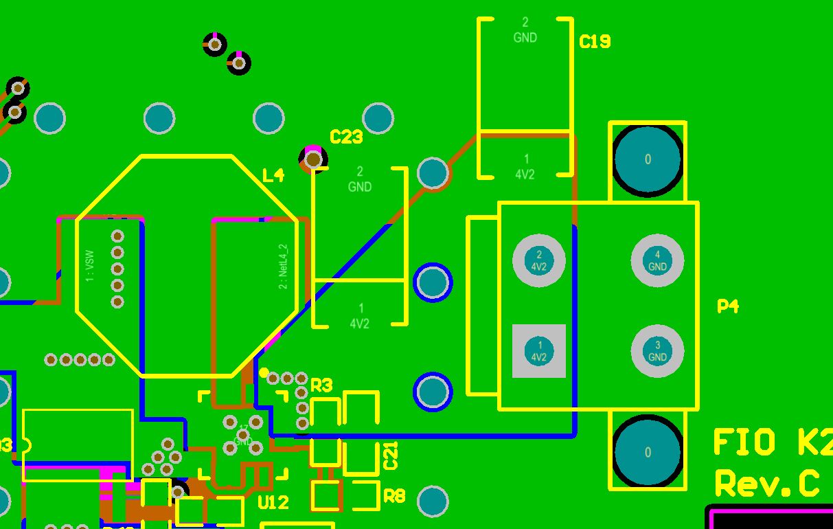
I have a circuit where, since the design released, I have had users whose TPS61030 has failed. This is a low volume design since it is part of a power supply on an evaluation circuit, however the failure rate is quite high, about 5 to 10%. The TPS61030 fails for no rhyme or reason. The TPS61030 itself shorts internally and remains shorted between the input power ( pins 1 and 2 ) and ground ( pins 3, 4, and 5 ). The thermal relief “power pad” doesn’t short though. The short is anywhere from 3 ohms to 35 ohms.

Does anyone have any suggestions as to why this may happen and what I can do to fix this?

I input 3.3V into the TPS61030PWP regulator and have designed it to boost up to 5.0V. The perplexing part about this is that there is little to no current draw on this 5V supply. It was designed to handle at least 300mA of power, but such current draw has never been necessary so typical current draw is theoretically zero, minus any leakage, to possibly 20mA. Due to such low current draw I doubt we can blame this issue on any excessive current. I have had two of these regulators fail in the last week and in neither case was I even using the 5V supply from this part – who knows, maybe that is part of the problem.

I do use the TPS61030 in sycnhronous mode, running at 520 kHz. The clock shouldn't be the reason, it is driving another separate and different power supply and there is no failure there. I have the power supplies synchronized due to this evaluation board's use of RF.

Thanks.

  • Typically, failures of boost converters are caused by poor board layout with excessive impedance between the Vout pin, output cap, and PGND.  Check your layout against the datasheet and EVM.

    I would recommend using a lower power boost in the future, such as TPS61220 or TPS6125x series.

  • Thanks for the reply, Chris.

    The layout did take into typical switching power supply layout methodology. The capacitors are very close to the output pins.  VOUT is laid out using a copper pour from the pins to the capacitors with less than 2.2mm if signal travel. In addition the capacitors are ceramic, I have two 100uF in parallel and they have 30mOhms of ESR each according to the datasheet at my switching frequency and subsequent few harmonics.  I am also using the adjustable version of the device which TI suggests because, well, I prefer to use adjustable parts but TI also recommends to do so if I used ceramic capacitors.

    Do you still believe there is an impedance issue or have something to suggest after considering the additional information I have provided?

    Thanks.

  • Not only the Vout connection to the output caps is critical but also the ground routing.  Compare your layout to the EVM.

    Ceramic capacitors do not have that much ESR.  This IC really works best with tantalum output caps that have some ESR.

  • I am suffering from the same issue. several board got input short on TPS61030 without clue. I have been debugging this for months. We did ESD, over current test, but just could not duplicate the problem in lab. But field keep report the this failure.

    Why the booster input could be short? Could it be the high current on the output side?

  • Input is 2.7V~4.4V

    My board has 330 + 470uF TAN cap on the output side, 100uF on the input side. The normal current is 400mA and peak current goes up to 2.5A.

    Solid ground plane, power path is cover with wide copper.

    Under what type circustances, that internal FET will constantly conduct and finally burn? Or what could trigger the input short to GND? If you need, I could send you the sch and layout.

  • You need to compare your layout to the datasheet recommendations and EVM, as I recommended to the previous person on this thread.  The output cap must be placed closest to the IC and routed directly to its pins or else parasitic inductance will cause voltage overstresses that destroy the device.

  • Thank you for your quick reply. In our design, we used wide coper in three layers to conduct the output. There are 6 vias right after the tps61030 output pin that connect three layers together. And 330uF+470uF are connected after the vias, only 3/16 inch away from output pads, same distance as EVM.

    So compared with EVM, our output path shall have less impedance because it has three layers, and on each layer, the trace is wider than EVM. And we had bigger Tantalum capacitors are as close as EVM. The only uncertain part is the vias.

    Has another customer run into similar problem and they fixed it by routing? I just want to make sure that after several months of debugging, we are deal the root cause this time.

  • You also need to have a 2.2uF ceramic on the output, closest to the device.  This is required for the snubbing action.

    The tantalum caps should also have an ESR in the datasheet's required range.

    Yes, most failures with this IC are layout related.

  • Hi Chris:

    We had 2.2uF ceremic cap beside the pad.  Can I send you a snap shot of our layout for review? I don't see any problem in our layout.

    Does all reported failures show short input? Is there a way I can duplicate this failure?

  • Sure, you can post your schematic and layout in this thread.

    Most of these failures show shorts on either the Vin or SW pins.

  • Thanks for posting this.  Your output caps just seem too far away.  Swapping the small ceramic with the top FB resistor would have gotten it a lot closer and the tantalums are nowhere near the IC and their routing is round about.  You also need a small ceramic on the input.

    I recommend that you order the EVM, modify the divider to get 4.2V, and then wire it into your circuit to continue your testing.  When everything works ok, then you can copy its design onto your new boards.

  • Hi Chris:

       Thank you for your suggestion. I want to understand the root cause of the failure. Is the overshot on the SW (Absolute Maximium 7V) cause the issue or unstable output voltage cause internal logic fail. Our product are in the production, and I had never seen this problem in house. And then this booster failure came in almost every two weeks since May. And we are re-spining the board, trying to fix the issue. But I am not confident that layout could 100% fix the problem unless I fully understand the root cause.

    We had two EVM in house. I could not duplicate this problem in house.

    I had comared the cap distance and pulse on the SW pins. With same load (4Ohm, ~1A), EVM has 7.1V overshot on SW and our board has 6.4V overshot. I am not sure if this can prove that our board is performing better?

    In short, my questions are:

    What is the root cause of this issue? I understand that no company is willing to expose product issue. But we need to understand the issue before we can take correct mitigation.

    Is there a more resilient part that has similar feature(peak current 4A) or updated version of this part?


    Thanks,

    Hongtao


  • Hi Chris,

    I am the contract engineer responsible for the PCB layout design in question. While I completely agree that proper layout is critical, I don’t think this is the case with this particular layout. I think you may have misjudged the placement of components and connections due to lack of scale on the plot you reviewed and you also could not view the solid GND pour on the bottom side of the layout.

    For more detailed review  I am attaching to this post a brief comparison of the output capacitors connection on the EVM versus the board we are trying to fix.

    Please note that our second tantalum capacitor C23 is optional, and it’s not equivalent to your dual cap placement on the EVM. Our original design configuration uses C19 to substitute for the dual caps (C1+C2) on the EVM. All connections are made on polygons, not traces, with current paths which are the same or shorter than the ones on the EVM. Finally, all the connecting polygons are implemented on the outer layers of the board with 2 Oz-in (which is most likely 2 to 4 times the thickness on the EVM design). Our overall ESR is significantly lower than that of the EVM and so is the resistance/inductance of the      

    The question we have is with regard to the failure mechanism in play here. All we know is that following failure the IC output shorts to GND with low impedance, but it’s not clear what could be causing the failure.  Hypothetically, if we rule out the PCB layout as the root cause, what kind of additional measures can we take to avoid this failure?  

    For example, if the internal over voltage protection is inadequate should we clamp the output with a fast TVS to avoid high voltage spikes? Or if the internal short circuit protection is marginal, should we limit the output current with a fast current monitor that will shut off the regulator supply in case of short?     

    Thanks,
    Gil Elgez.

    Link to attachment:

    http://e2e.ti.com/cfs-file.ashx/__key/communityserver-discussions-components-files/196/2703.EVM-to-FIO-PCB-comparison.pdf

  • Ah, that this design is in production changes things quite a bit for this situation.  You really need to work with your local TI or distributor FAE.  They can work with you to look at the details of your product and how the customer uses it to get to the root of things.  I think it impossible for me to that here.

    The most common root cause of failures on this IC that I see are layout related.  Poor output cap placement.  I listed some improvements to your design that would be good to incorporate into a next rev of the PCB.

    But since you didn't see any failures during development and are now seeing field failures seems to indicate one of two things: either the product wasn't tested enough or in the way the customer will use it during development or the customer is using it in an unintended or untested way.

    Building up your schematic on the EVM and measuring and comparing the same signals is an excellent way to judge your board layout.  Yes, overshoots on either SW or Vout are the most common root causes of layout induced damage.  You need to be sure and measure right across the IC's pins, with full bandwidth, and using a low inductance probe to make sure that you are comparing the real waveform and apples to apples.

    Other items to look into would be any kind of overshoots on Vin during power up or if the battery is plugged in/out for example.  Also, look at the output side of things and see if there is any way that the user could make contact with (i.e. touch) any nodes or apply an overload or short or apply an external voltage, etc.  Finally, check your inductor's saturation current rating and make sure it is sufficient for your application.

    There are no other currently available 4A boosts, though there is the TPS63020 buck-boost converter.  You can use the power quick search at power.ti.com to see if there are any other converters that meet your Vin and Vout needs.  With 1A load current, you might only need a lower switch current device such as the TPS6102x family or TPS6125x family.

    There are no issues with this device, when used with the proper layout and external components and within the recommended operating conditions.  Note that there is no OVP in the device.  Adding a snubber or TVS on the SW pin or Vout net is done by some customers to reduce the ringing and/or EMI but should not be necessary at 4.2Vout.

  • Thanks for the information. That's very helpful. Two more question which might help us to identify our issue and find proper mechanism to prevent out failure.

    1. Why would overload or short on the output side could damage the input, causing SW short to GND.  We might have scenarios that output is short or overloaded. But I had tested in lab, overload the TPS61030 output with 4 ohm (1A), 2 ohm(2A), 1ohm (4A) and short to GND, I don't see any problem so far. Is it because the transition in the current will cause the inductor generate high spike on SW pin? Or something else cause the input short in this case?

    2. What is the criterial for over voltage on SW and output? Let say if we apply a TVS, which voltage should we clamp to?

    Thanks,

  • Yes, the device has over current protection built in but it's still not wise or recommended to allow the user to do things to the output that might trigger it, if they are able.  For example, one might be able to devise a circuit with inductance or other parasitics that repeatedly shorted and opened the output, causing the output voltage to vary constantly.  In theory, some random output waveform might interact with inductances, etc. on the PCB and cause overshoots on the IC.  This is just one area to look into--does the user have direct access to the output of the device to which they could do something harmful?

    The absolute maximum ratings are DC ratings that should not be exceeded.  We do not specify AC ratings.  So, to be safe, you'll want to keep the voltages below those in the abs max table.

  • Customer do not have access to the output. So they could not inject any thing, like suge, ESD or wrong voltage to the output.

    We connect the TPS 61030 output to a phone battery input(The phone shutdown at 3.6V, we want the system shutdown at 3.0V). We boost up the battery output in order to utilize all the energy from our battery. Phone load is not constant, depends on the user scenario, and wireless communication. The current varys from 100mA to 2A.

    There is one failure case that something was shorted on the phone battery input side (Booster output short). I am not sure if TPS61030 SW short is the result of output short

    All the other failure cases, I did not find any short on output side. So could it because the fluctuation of output current?

  • No, a changing load current will not destroy the TPS61030.

  • These new posts have rekindled my interest in this failure. One of the first points everyone is recommend to do is consider an error in the layout. My layout is very similar ( not the same, but similar ) to the TI Evaluation Board and yet I get these shorts. Here is a quick screenshot of the layout. I rotated the image so it conveniently matches the orientation used in the EVM datasheet.

    Cary

  • My upload didn't work. Trying again.

    ( The last attempt to upload E2E seemed to have started a new Post Thread, sorry. An E2E site manager can fix that up. )

  • I deleted your other thread.  No worries there.

    Your issue is likely the two ceramic output caps.  Ceramics don't have any real ESR.  This IC requires ESR to be stable.  The datasheet also recommends a small ceramic in parallel with the bigger tantalum.

    Your layout is very good, but with thermal reliefs.  These narrow traces and increase impedances and are not desired.

    I would retest with a 2.2uF ceramic at C208 and a tantalum with some ESR at C207.

  • Hi Chris:

      I uploaded the updated sch and placement. I highlight the change we made. Please have a look if there is anything we need to improve.

    TPS61030.zip
  • This are good improvements.  You might add a placeholder at least for another big input cap on the Vbat side of the IC.  Q3 presents some impedance to the device which might create unwanted input voltage ripple.

    Make sure the routing is done well and direct on the output caps.

  • Chris,

    I am using one of these parts in one of my designs and am having the exact same issues with failures in the field.  I am having a difficult time believing that all of these customers' issues reported in this forum are due to poor layout or component placement.  This really sounds like an issue with the TI part.  I see that you recommend calling an FAE.  Has anyone here done that yet?  Does anyone have any feedback from TI regarding the robustness of this part?

    Landon

  • Hello Chris,

    This is just a follow up on this issue:  We stepped up our production PCB revision and this time we carefully routed the TPS61030 circuit to follow up the same component placement, routing topology, and polygon structure as recommended and implemented on the TI evaluation module of the TPS61030RSAR.

    I am sorry to report the same problem occurs even under an ideal and recommended PCB layout.

    I am in the process of testing every board in the pilot run of the this PCB revision and will have better statistical figures shortly.

    At this point I am convinced this failure mechanism, as observed by many other customers,  can not be  resolved and is not entirely due to poor PCB layout.
    There is a fundamental component failure mechanism which is internal to the TPS61030.

    Gil.

  • You can post your new layout but the device has been qualifies to operate within the recommended operating conditions reliably.

    Poor board layout is the most common applications issue with these devices but other things might cause it to fail.  Such as input overshoot from a 'hot-plug' event, wrong inductor selection with too low of a saturation current rating, ESD, etc.  Your local FAE can understand your system and debug this with you.

    You are of course welcome to use a newer, easy to use device such as the TPS61200 or TPS6125x series.

  • Has anyone had anymore luck with this TPS61030 input shorting problem ?  I have the EXACT same problem on 3 different (careful) layouts !!!!

    I have also seen the problem on two different package types !


    Bill

  • Hi Bill,

    After multiple layout iterations and layout analysis, we spent almost a full day of work with a field application engineer from Arrow/TI on this problem.

    We carefully scoped the overshoot and undershoot switching/ringing on the SW pin and found out that even on TI's own evaluation board (and on any other layouts we tried) the maximum voltage ratings for the pin are being violated.

    We mitigated the problem by placing a (4.7nF + 2 Ohms) Snubber circuit from the SW pin to ground to reduce the ringing amplitude on the pin. There is a trade off with reduced efficiency after placing the Snubber circuit, but it should prevent the part from burning up.

    Gil.


  • Hi Gil .... Thanks for the speedy reply !

    So did you have that circuit in place all along and changed the values ?  How did you come up with them ?

    I have the components there, because they are in the datasheet, but I have a 10 ohm res and 1000pf cap.

    Can you suggest a good test after inserting the snubber ?

    I have this product going into the field for test in April and it makes me VERY nervous !!

    Are you going to continue to use this part ?


    Thanks !!!!


    Bill

  • Hi Bill,

    We came up with the Snubber values mostly by experimentation.  You'll have to try and find the optimum values that work for you. It depends how important is the overall efficiency in your application. Increasing the capacitor value would reduce the over-ringing at the cost of energy being dissipated on the snubber on every switching transition.


    The values I provided (or similar combination) could be a good starting point. In terms of power absorbed by the snubber, a 0603 resistor and 0603 capacitor series combination would do fine right next to the SW pin. Use an NP0/C0G cap if you can. In the initial experimentation we just soldered the snubber right between the pin and ground pour next to it. For our last production run we re-routed the board (for the 3rd or 4th iteration). We also thought of using a fast SC diode to absorb the undershoot, but I don't think it helped much.

    Probing the problem and the effect of the snubber could be very tricky. The switching transition slew rate on the SW node is very high. You'll need to use a high speed scope (high bandwidth amp and probes >200MHz). I soldered a custom probe-end (basically 1:1 coax stripped to 3mm length) right on the measurement node and GND next to it.

    TI is in deep denial when it comes to this part, somewhat understandably, considering how many people went to production with this part and ended up with significant production yield losses.

    We no longer use this part for new design. There are very similar parts from TI that can be used as replacements, especially if you don't need the maximum current output capacity.

    Good luck and please post here to share your findings for better or worse,
    Gil.


  • Thanks Gil for sharing your experience.  Even after all these years, this is still a popular part for our customers.

    Bill, here is our snubber app note: http://www.ti.com/lit/an/slva255/slva255.pdf  The values almost completely depend on the parasitics on your board, so you'll need to tune it in the lab.

    I would also recommend using a different device if your power needs allow it.  We have many.  Our TPS6125x series is our latest generation of boost converters that is much more integrated and reliable.  And check back often.  We release new devices frequently.

  • Hello,

    I have the same problem. IC fail without ny rason.
    Did you find solution?
  • Hi Biser,

    Please read discussion notes above. We tried to use a snubber but lost efficiency. That was a few years ago...I can't recall the exact details. 

    Your best bet is to use another part and avoid the TPS61030 in favor of a higher power replacement. 

    Gil.