This thread has been locked.

If you have a related question, please click the "Ask a related question" button in the top right corner. The newly created question will be automatically linked to this question.

LMZ10500 Failure and Damage

Other Parts Discussed in Thread: LMZ10500, TMS320DM368, LMZ10501

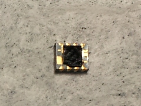
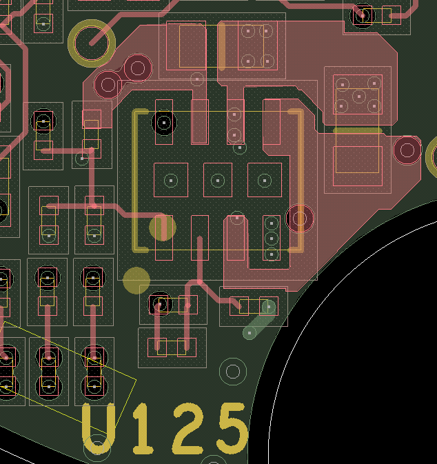
I am having a recuring issue using the LMZ10500 in two locations on a prototype PCB.  Can you help determine why these parts are being damaged and assist us in fixing them?

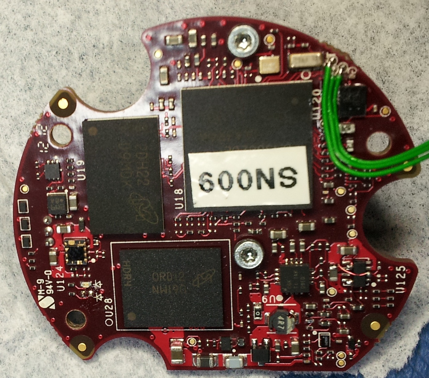
U125 is setup to generate 2.8V and U124 is setup to generate 3.3V.

1) In the case of U125 the part fails at almost 100% immediately after intial power up.  The failure exhibits the following:

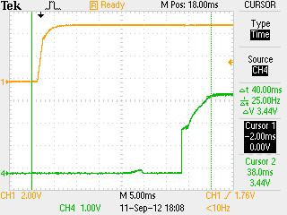
  • Vref  pin is not reaching 2.35v.       
  • VREF pin is hovering at around 0.3V output wanders around 0.7 to 1.5V
  • Vcon pin is 0v. 
  • Part is getting hot.
  • The part fails again after replacement.
  • We replaced this part with an LDO as a stop gap work around and this works fine.
  • I have lots of failed parts that could be tested if that helps.

2) In the case of U124 the part fails after many hours of operation

  • In general the part is hot and the output is 1.8V or so.
  • I don't have the failed parts in hand at the moment for other measurements.
  • The primary difference in the configuration of this regulator is that it has a diode on the output as per the design recommendation of the the TMS320DM368 which this is powering.
  • When replaced it will operate from days to weeks with no issue.
  • We are investigating an LDO replacement.

3) Will oscillation on the Enable pin during startup cause damage to the part? This has since been fixed but not on the boards that have failed and not tested long enough to not fail.

4) If there is 0.3 to 1.8V on the output after VIN is applied but before EN is high will this damage the part?  This appears to be present due to leakage rom teh TMS320DM368 in our system.

Please see attached schematic: 0003.falconeye_fl-fv02-001_schematic_X12_2p8Vsnippet.pdf

And BOM: 2018.FALCONEYE_FL-FV02-001_BOM_revX13_ver2_LMZ10500parts.xlsx

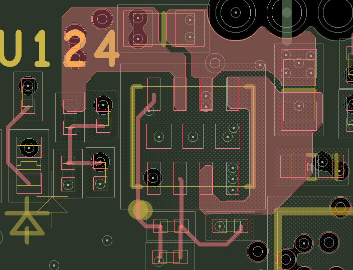
Note C473 and C474 are shown incorrectly on the schematic and have been placed across R586 and R589 on the board as a modification.

U124 Layout

U125 Layout


Thanks for the help in advance!

Jason C

  • Hello Jason, 

    Thank you for the detailed description, schematic, and board layout snapshot.

    Here are a few more questions to help us start debugging.

    1. Do you have any scope shots across the input voltage terminals of U124 and U125 as the input rail is ramping up to 5V? Also, it would help to monitor what the EN pin voltage looks like during the startup sequence. I am hoping to rule out any overshoot/oscillation above the abs max input voltage and also on EN voltage with respect to VIN.

    2. If you look at the bad units under magnification, do you see any physical damage to the die on top of U124 and U125? I am hoping to rule out damage done during assembly/handling.

    3. You mention the units are running hot. Is this at room temperature? What is the maximum load on each of the two rails and what is the overall board size? Is the ground plane layer in the board layout on the bottom layer or internal layer? I am trying to get a feeling for the expected (normal) junction temperature for this design.

    4. Could you take a picture of the assembled board and attach it? It can be just the section shown in the board layout shapshot you provided. 

    Thank you for the clarification on the C473/4 cap placement. Yes, these should be connected from the VCON pin to GND.

    Regards, 

    Denislav

  • Denislav,

    Thanks for getting back to me quickly.

    1) Overshoot: I am having the scope shots ordered up so that it is easily shown on one shot.  I have other shots and haven't seen any overshoot.  The regulator is fed through a FET softstart circuit.  I have recently made a change in the enable for the first regulator in the startup sequence to delay enable until after the softstart time is complete as the softstart action was causing oscillation in the first regulators PG output. 

    a)  Basically 5V from USB through a FET sofstart comes up in about a 20ms monotonic ramp with no peaking and feeds these parts.  Nominal is 4.5 to 5.5V as per USB specs.

    b)  The enable comes from the 1.8V regulator and remains low the entire time until the 1.8V power good is released about 5ms later.  This PG has a weak pullup to 1.8V which is probably not necessary.

    2) Damage:  I have found units with Damage including the latest one received on Saturday SN009 had damage shown below. 

    a) See below assembly as well U124 is on the left of the board before removal.  U125 location is on the right but has been replaced by an LDO. 

    b) I have recectly become aware of the mounting and rework guidelines for these parts and have communicated them to our manufacturing folks. 

    c) I will look back through some of the damaged parts and look for other signs of damage.  We will also keep an eye out for further damage. 

    3) Yes we are just at room temperature when malfunctioning they are very hot to the touch such that you can't hold your finger on it more than a second. 

    a) When operating normally there is no heat at above the board ambient. 

    b) The load appears to be about 100mA during idle operation and could go as high as 250mA. 

    c) The ground plane is the next layout down below the external copper layer these are mounted on and is full extents of the board.

    4) Assembly: Here is the board assembled.


    Thanks!


    Jason C.

  • Hi Jason,

    The bad unit shown above has severe physical damage. The question is whether the damage occurred during removal of the unit or initially during assembly. Please inspect some "freshly" assembled boards to see whether the assembly house needs to make adjustments.

    Here is some guidelines you can pass along to the assembly house:

    Use the following recommendations when utilizing machine placement:
    • Use 1.06mm (42mil) or smaller nozzle size so that the nozzle head does not touch the outer area of the exposed die.
    • Use a soft tip pick and place head.
    • Add 0.05mm to the component thickness so that the device will be released 0.05mm (2mil) into the solder paste without putting pressure or splashing the solder paste.
    • Slow the pick arm when picking the part from the tape and reel carrier and when depositing the IC on the board.
    • If the machine releases the component by force, use minimum force or no more than 3 Newtons.
    • For PCBs with surface mount components on both sides, it is suggested to put the LMZ10501 on the top side. In case the application requires bottom side placement, a reflow fixture may be required to protect the module during the second reflow.

    For manual placement:
    • Use a vacuum pick up hand tool with soft tip head.
    • If vacuum pick up tool is not available, use non-metal tweezers and hold the part by the inductor body side terminals rather than the micro SMD die on top.
    • Use minimal force when picking and placing the module on the board.
    • In case a heat gun is required for rework, make sure that the heat source is pointing at the interface between the inductor and the PCB. Do not apply heat gun directly on top of the component since it may affect the solder joint between the micro SMD and the inductor. Using hot air station provides better temperature control and better controlled air flow than a heat gun.
    • Go to the video section at www.ti.com/product/lmz10501 for a quick video on how to solder rework the LMZ10501.

    Regards, 

    Denislav

  • Thanks Denislav!

    The damage was apparent prior to removal from the board but it is hard to say if this happened after assembly.  I am now taking precautions on both sides and we will put a peice of kapton tape over the part to protect it after assembly or rework.  The updated assembly guidelines have been sent to our manufacturing folks so hopefully that will take care of the other side.

    This part is one of the tallest in the location so when debugging the board with this part facing down there is risk of damage so I am hoping the kapton tape will help alleviate some of the problems. 


    1) There has been some discussion of encapsulation on this forum, is there any update on recommendations with that?

    Here is the scope shots that you requested earlier:

    2)  The scope shot below shows the 5V input in orange to the board versus the Enable to the part in question U124 in green.

    3) The scope shot below shows the 5V input in orange to the board versus the Output to the part in question U124 in green.


    Thanks!

    Jason C

  • Hi Jason, 

    Instead of tape, if you are not using the screw holes on the PCB you could insert some standoffs when working with the board so that the part is not the tallest component. Also, another approach could be adding some sticky rubber feet (similar to the standoffs) to achieve the same result. 

    In terms of encapsulation, I know that we have tested conformal coating over the part.The coating that we have used is from Dow Corning P/N 1-2577. We have run temperature cycle and humidity reliability tests and all have passed.

    If you work with new physically undamaged unit, do you still experience the electrical misbehavior you were seeing before? 

    Regards, 

    Denislav

  • Denislav,

    We are using the holes currently for mounting an optical assembly so for proto the Kapton tape plus a little extra care seems like a good option, let me know if you can think of a better way for use on the bench. 

    Encapsulation is probably a better approach for a manufacturing solution but we will need something that can encapsulate just this section of the board.  There are other partsof the board which cannot be encapsulated.

    I have not found a device in this U124 location that has failed but appears undamaged.  We will keep an eye out for any parts that seem undamaged yet are misbehaving.

    Thank you for your help!

    Jason C.