This thread has been locked.

If you have a related question, please click the "Ask a related question" button in the top right corner. The newly created question will be automatically linked to this question.

DC/DC converters shutdown mode

Other Parts Discussed in Thread: TPS61085, TPS5450

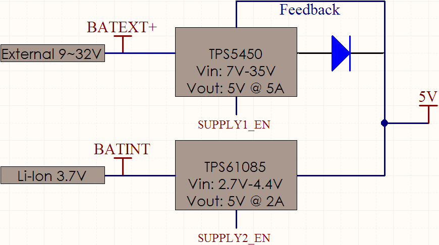
I'm developing a new design in which I'm probably going to use multiple power sources (with different power controllers) and in this design I got a doubt I wasn't able to find in the datasheets of the components. I guess this must be something generic for most DC/DC controllers.

Now the question: when I put one of those converters in a shutdown mode using the enable (or shdn) pin, what are the states of the IC input and output pins, do they go to a HiZ state? In that state, is there any further isolation between the IC pins and the external environment? And between the input and the output power pins?

Thanks in advance for the help!!

Best regards,

Breno Rocha.

  • You will have to provide part numbers.  Different devices behave differently.  In general, just the switching node is inhibited from switching and also the SS pin is usually discharged and held low.  If there is a PWRGD pin it may indicate "out of regulation" or it may be inactive.  It will all depend on teh specific device.

  • The parts I'm considering are TPS5450, LM2841X and TPS61085. My main concern is with the Vout and feedback pins, which may have power connected (I believe there will be no problems with Vin).

    For the Vout, I'm considering the use of a series diode after the inductor, conecting the feedback reference after this diode, so I can still have the desired voltage. That would block current flowing inside the converter.

  • I dont actually support any of those parts, but I know the TPS5450 pretty well.  It does not actually have a VOUT pin, but when EN is held low the device is not switching, so the output and the fed back portion at VSENSE will be 0 V.  The error amplifier is active though as long as power at VIN is applied.  I guess I really do not understand your concern.

  • The thing is that I'm cosidering the connection of two power supplies in the same line (i.e TPS5450 and TPS61085), a buck that will power the circuit from an external power supply and a boost converter that will power the circuit from a 3.7V, Li-Ion battery (regarding current, the circuit will consume less current in battery mode).

    So, in summary, for the feedback pin, there will be no issue, as although the error amplifier is active, the feedback comparator reference would be 0. The VOUT I'm refering to is the PH pin, which is the source of the high-side fet of the converter (where the inductor is connected), and, for that one, I'm considering the use of the diode.

    The image below shows the connection I referred to:

    Thanks for the help, and sorry if I wasn't clear enough.