This thread has been locked.

If you have a related question, please click the "Ask a related question" button in the top right corner. The newly created question will be automatically linked to this question.

Noise in UC3823N

Hi,

I used UC3823N in my boost converter to work in CCM voltage control mode. However, it turns out that converter works in DCM and output voltage is much below it's designed. I checked the output PWM and Ramp signal on pin 7 as picture below

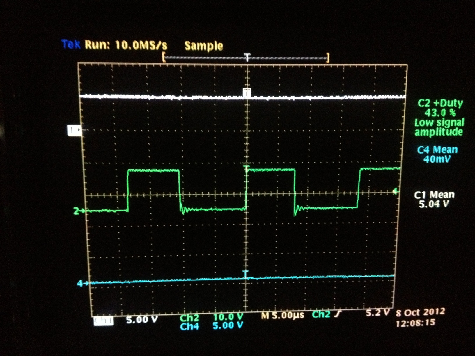
The white line is output PWM of UC3823N, the green line is output voltage of converter.

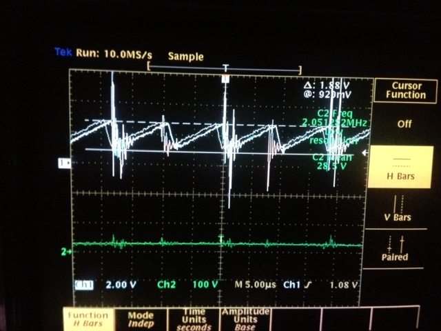
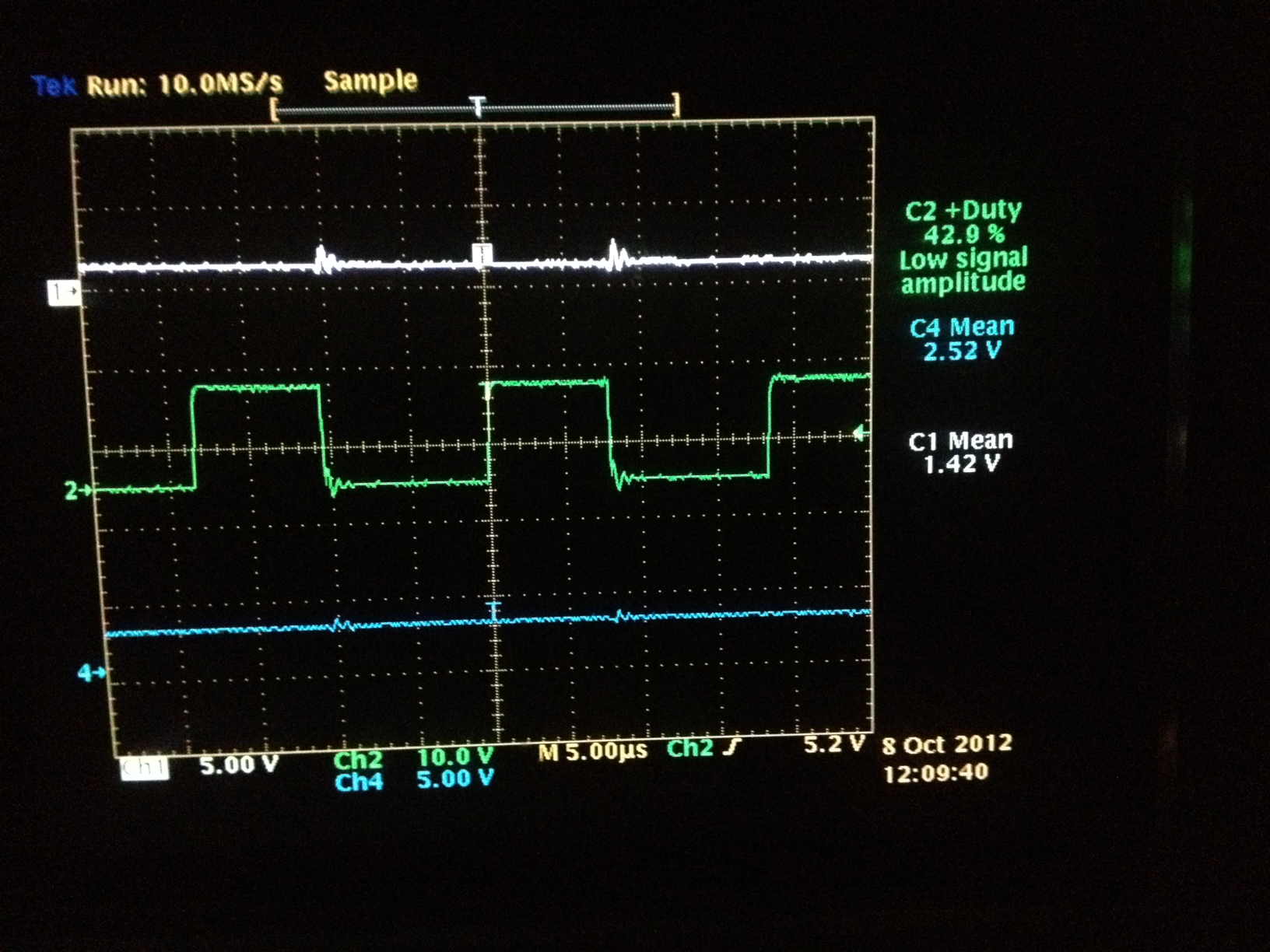
The white line is ramp signal of UC3823N, green line is output voltage of converter.

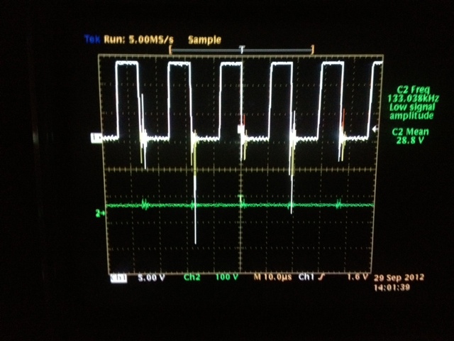
I think it may be the noise that cause my circuit works in DCM,  can anybody help me with this problem?

  • DCM usually happens under lighter loads, DCM operation is typical when the load current is less than 1/2 the inductor p-p ripple current. You could try increasing the inductor to get it to stay in CCM.

    Regards,

    Rachel Coulter

  • I forgot to mention, if you increase the inductor you should reduce the output capacitor the same way, then the crossover frequency and compensation can stay as they are.

  • Hi, Rachel Coulter.

    Thanks for your reply. According to my calculation, the critical inductance is about 23uH, I choose 50uH in my converter, I don't think it is because of lower inducatance that makes it work in DCM. I tried heavy load, it still works in DCM and output voltage doesn't meet reqirement(much belower than design). I tried to use funcation generator to have 75% duty cycle PWM, however, this makes boost converter works in CCM and has right output voltage. So I think that maybe something goes wrong with my control chip(or compensator).

    Herer are the parameter of my converter: input voltage 12V, output voltage 48V, input inductance 50uH and output cap 220uF.

    Regards,

    He, Siyu

  • He, Siyu

    Thanks for the additional information. Could you provide probe values at some of the pins? specifically the current limit pins (11 and 9) as well as output PWM and output voltage pins etc.

    A schematic would also help trouble shoot the issue as well.

    Regards,

    Rachel

  • Hi,

    the below is my circuit schematic

    The next one is probe values

    The white line is pin 11(current limit), which I conneted to Vref(Pin 16, 5.1V). The green line is output PWM. The blue line is pin 9(Ilim/SD) which I connected to ground, because I used voltage mode control.

    The below is pin values of inverter input and noninput of error amplifier

    The white line(1.42V) is feed-back input to pin 1(INV). The green line is output PWM again. The blue line is input to pin2 (N.I.)(2.52V), which is connected to voltage divider(half) of Vref(pin 16, 5.1V).

    Regards.

    He, Siyu

  • Hi,

    My consideration is that the input voltage of INV(pin 1) is much belower that N.I.(pin 2), why doesn't output PWM duty cycle go up? Instead, it stays at 43% duty cycle.

    regards.

    He, Siyu