This thread has been locked.

If you have a related question, please click the "Ask a related question" button in the top right corner. The newly created question will be automatically linked to this question.

BQ77908A configuration file (*.cfg) format

Other Parts Discussed in Thread: BQ77908A

I am attempting to program a BQ77908A using a USB-TO-GPIO interface with version 2.0.19 firmware, but can find no reference in the documentation defining the format required for the configuration file.   I have sucessfully installed the BQ77910-BQ77908 Programmer software and the device connection is made, but when I have attempted to load a file with the configuration data I get exceptions or file errors.    Please provide an example of a properly formatted configuration file.   Following is one of my attempts assuming that a semicolon would terminate the input info (all data following the semicolon seen as comments???), but it does not work.

0xcc; 0x1 – SYS_CFG -                     4-series cell configuration, thermal detection in all modes, recover OT fault requires load removal, recover OCD/SCD with load removal

0x26; 0x2 – OV_CFG -                     1Over-voltage trip voltage of 3.75V

0X52; 0x3 – OV_CFG2 -                  Do not use TS for external charger control, over-voltage hysteresis of 50V and over-voltage trip delay of 1 second

0x06; 0x4 – UV_CFG1 -                  Use hysteresis (see below) and trigger under-voltage level at 2 volts

0xc4; 0x5 – UV_CFG2 -                   Load removal required upon UV event, shutdown after 8 seconds, hysteresis of 0.4V, under-voltage delay of 8 seconds

0x04; 0x6 – OCD_DELAY -              Over-current delay is 100mS

0X0f; 0x7 – SCD_DELAY -               Use lower range for current limits and fast delay setting, trip in 960uS for over-current discharge event

0xba; 0x8 – OCD_SCD_TRIP -      Short circuit discharge trip at 30A and over-current discharge trip at 15A

0xf7; 0x9 - SCC-CFG -                      Over-Current charge duration of 960uS at 45mV (9 amps)

0xed; 0xa – CELL_BAL_CFG -       Start balancing at 2.6V (cell voltage) during charge for a maximum of 4 hours.

  • The easiest way to get a working format is to connect to a part and save a file.  Then you can edit the file to generate multiple files

    In general it will ignore blank lines or treat any line with a semicolon as a comment.  So you can't have in-line comments, but you could add a comment line or lines above or below the value.  Registers and data are in hex on individual lines with a colon in between.  An example from a saved file is below, this may not represent a suitable working configuration:

    ; bq77908 Register File
    ; 1/27/2012 9:52:11 AM
    01:4C
    02:39
    03:42
    04:C
    05:C1
    06:10
    07:F
    08:0
    09:F0
    0A:F3

  • Thank you!!!

    The file is loading properly now that I have the correct format.

    Now I am experiencing a "Program Failed" message.   I note that the ZD pin is strobing a momentary voltage (using DVM) [I need to get a scope at my office desk where the programming software is installed], but the PGM pin does nothing (0V continually) which means that the 14V programming voltage is not being gated to the EEPROM pin of the BQ77908A.  Is there any explanation on the operation of the programming interface protocol, e.g., is ZD supposed to stobe which is what I would expect the PGM pin to do???  Does the data get written and then read for validation?   What is the nominal clock clock rate for ECLK?   The header diagram of the EVM schematic on page 30 of the EVM Evaluation Manual shows pin 1 in the upper right corner whereas when looking at the header from the top of the EVM and my design, pin 1 is at the upper left, i.e., the diagram appears as if the header is being viewed from the bottom.   I connected the header pins by their name (pin number) and not by their represented location on the page even though the odd and even pins appear swapped? 

    The programming interface circuit I have constructed is a clone of the EVM schematic on page 30; I did not include the three-terminal header marked "Install shunt for test" as the EVM instructions indicate to remove this strapping option.   The ZD pin is pulled down with a 100K ohm resistance so there is little load on this pin.  There is no separate driver on the ZD signal.

    I have used different USB_TO_GPIO pods, different programming modules, and different target boards with no success at programming.   Since I did not have room on my target board for all the programming components, I placed the J2 (2-pin header), J3 (10-pin header), Q1 (BSS84), Q2 (BSS138), C1, C4, R1, R2, R6, R8, R9, R10, R13 and R15 on one PCB and via a 5-pin interface (EEPROM, ZD, ECLK, EDATA, GND) placed the other programming interface components on application PCB so that pulled downs and zeners would be present on the open signals of the common 5-pin interface when disconnected from the programming module. 

    Any suggestions as to what I may be doing incorrectly?


  • Thursday morning update.

    Now that I have a scope I can see the ECLK rate of about 50kHz, but I am only getting what appears to be only 6 clocks pulse trains of 9 clocks each (3.3V in amplitude), but I would assume I should see at least 10 pulse streams, one for each of the 10 programming values.  The clock pin does appear to be correct (9 clocks), so I believe my header connection is not reversed (odd for even) as I first expected.   The ZD strobe is 43mS in length with an amplitude of 3 volts.  The PGM pin from the USB-TO-GPIO pod does nothing (0 volts continually).   The EDATA trace does appear to be data with the first byte being 0x20 (ASCII space) which does not correspond to any of the data from the file and not the first entry of 0xcc which I may expect unless the protocol has some preamble associated with the data sequence.   If the ninth clock is an ACK, it is high which means NACK if the protocol follows the SM Bus methodology.

    Hope this additional info helps.    Thanks for your assistance.


  • A scope should help.  If you also have an EVM you might do some signal comparisons.

    The ECLK should be ~ 50KHz as you observed

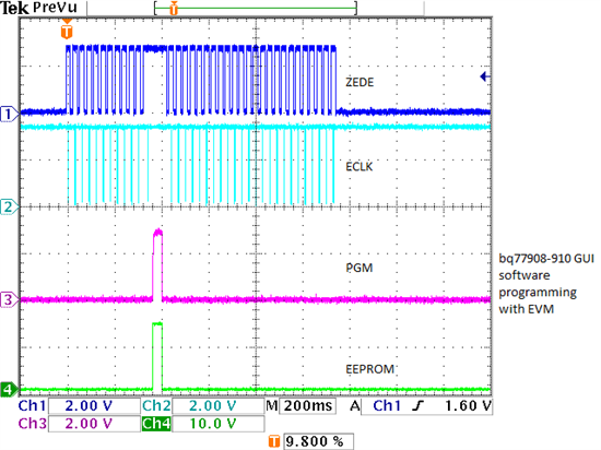
    ZD and ZEDE should pulse high during the communication.  If ZEDE does not go high the part won't ack. This would show up on the scope.  In the GUI check the status on the bottom left to see if it indicates success or NACK.  Also messages may appear indicating it can't find target or communication lost.

    The update sounds like signals are getting to the board but the sequence stops.

    Certainly check the pinout of the connectors and signals to the IC.  The USB-to-GPIO and EVM board use the industry standard pin layout.  The schematic symbol may be flipped and rotated for convenient signal exit for the symbol and is not meant to be a top side pin view.  Also check for the common assembly shorts/opens/solder/wrong components.

    The bq77908-910 software is not strictly like the datasheet programming flowchart in that it is an evaluation tool.  The registers are written as values are changed.  When the programming command is selected, the volatile registers are read and compared to the GUI values, if they don't match the sequence stops and there is a message box.  (If the part does not respond it should also stop).  If the verification was successful it will continue to write control registers and switch the PGM signal to control the EEPROM voltage.  After the programming the registers are verified. A successful programming sequence with the GUI and EVM looks something like the following

    Check to see if the part is powered.  The USB-to-GPIO provides pullups from its power supply, so presence of signals does not indicate the '908 is on or working. Also be sure the CHGST pin is held high during the programming cycle, it is not provided by the USB-to-GPIO.  If the part shuts down between the volatile register write and the programming command the register value match warning should appear, if it shuts down during the programming an unsuccessful programming message should appear.

    The GUI error messages are meant to be descriptive and may give guidance as to whether there is a basic communication problem, a data verification problem or a lack of verification after programming.  The description yesterday sounded like the part talked initially then failed to verify after programming.  If this is the case check for shorted/missing PGM, 14V supply and ground, or poor rise time or droop of the EEPROM signal/switch.

  • Programming is sucessful!!!   Thanks!!!!   The "gotcha" was that I did not have the CHGST pin pulled to PACK+ via a 15K resistor during programming.  The programming instruction (SLUA648–July 2012) indicates "Before running software, some hardware connections must be made to assure the necessary signal can be applied to the specific pins of bq77910 or bq77908 from the USB-TO-GPIO tool kit, for details on which signal should connected, refer to schematic of bq77910EVM in document  sluu368."   The required connection to CHGST is lost in the schematic, but for future releases a reference to Figure 3 would be helpful.

    For testing I "reprogrammed" the over-current discharge, over-current charge and short-cicuit discharge to the minimum values of 5A, 8A and 2A, respectively based upon the 5 mohm sense resistor being used   See registers 8 and 9 below.  The ISNS_RNG bit is 0 in register 7 (bit 5) . 

    01:CC
    02:26
    03:52
    04:6
    05:C4
    06:4
    07:F
    08:00
    09:F0
    0A:ED

    However, upon testing we could could charge at 3, 4 and 5 amps and discharge at 6 amps without protection being invoked (we need to improvise to get a controlled short circuit current as our load box is maxed out).  We measured -15mV across the sense resistor during the 3 amp charge sequence.  Any ideas as to what we did wrong?  Are there any special procedures in reprogramming the device with new values?   Is there any way to read the register values after they have been programmed?

    Thanks again!!

  • Glad you had success, and thanks for the suggestion.  The programming software associated with SLUA648 does assume a familiarity with the part typically gained from using the evaluation GUI and boards, sorry for the confusion.

    A scope may be very handy for looking at the current protection behavior also.  Be sure the part is not protecting and recovering so quickly that it is not apparent.  Refer to table 2 of the datasheet or other detailed descriptions.  For example SCC will recover with CHGST low.  Also see http://e2e.ti.com/support/power_management/battery_management/w/design_notes/1380.aspx 

    You can apply a voltage from a supply through a divider to the sense inputs for initial checkout or a low voltage supply across the sense resistor or battery- to pack- current path.  This lets you do initial checkout without the high wattage power supplies and loads. Zero delay mode (ZEDE high) may help see trips if you think the load may not be constant, but it will also allow trip from noise.

    For long term data retention the number of programming cycles is recommended limited to 3, see the datasheet. In evaluation you might write a part many times, but may not want to put that part in the field. When you write register 0x0B back to 0x00 in the programming sequence, you can read the EEPROM values from the registers 0x01 through 0x0A.  The evaluation software will do this, not certain about the programming software.