This thread has been locked.

If you have a related question, please click the "Ask a related question" button in the top right corner. The newly created question will be automatically linked to this question.

TPS5450 webench calculation right? device will be to hot

Other Parts Discussed in Thread: TPS5450

Hello Dear,

I have some Problems with the device.

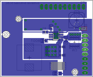
Attached you find the webench design. Can you tell me if I use these parts in this report, then i can get 5A at 12V at the output?

The Inductor seems a little big with 47µH...

By the last test the device became very hot more than 110°C how it can drive 5A over a longer time?

8176.WebenchReportsServlettps5450-02.pdf

  • I calculate 10 uH as the proper inductor value.  The webench tool may have adjusted that to allow for a suitable output capacitor that can provide stability as well as the required ripple current rating.  Since the TPS5450 is internally compensated, you have to have some leeway to align the output filter double pole and ESR zero with the internal compensation poles and zeros.  As to your main concern, yes the TPS5450 will get hot at higher output currents.  that package is at the limit of its thermal capability at 5 A.  It helps to provide ample copper for heat dissipation.  It is best to provide that on the outside layers of your PCB, rather than an internal ground plane.  You can add some additional vias directly adjacent to the exposed pad area.  Also there will be additional power dissipated in the catch diode.  make sure to provide some thermal dissipation copper for it as well.  Then of course in your final design you will need to pay attention to your load.  12V @ 5A is 60 W.  If this is used as a point of load regulator, then you will be dissipating an additional 60 W nearby that can contribute to temperature rise.

  • Thank you for the answer.

    So i suggest to use the Inductor Würth 7443321000 10µH, rated current: 9A, saturation current 10A.

    I want to use the diode in D-Pak package type: 50WQ10FNPBF Vishay Semiconductor.

    1. Cboot Kemet C0805C103K5RACTU Cap= 10.0 nF

    2. Cin TDK C5750X7R1H106M Cap= 10.0 μF

    3. Cout Kemet T495D686K020ATE150 Cap= 68.0 μF ESR= 150.0 mOhm

    The layout is attached, all parts are on the bottom side. I have vias to the top side. There a heatsink will be mounted.

    Is the ground trace ok?

    I cannot change the place of the supply, ground and output pins.


  • I think the ripple current is too high to use 10 uH with that output cap.  I am a little concerned about the ground routing.  Most always the input capacitor must be tightly coupled to the VIN and GND pins.  The way you have that routed requires a long path from the VIN ground return to the IC ground.  You can look at the layout guidelines in the datasheet.  Also, with that diode you are heat sinking to the switching node.  Ideally you want to keep that node as small as practical, especially if you have noise or EMI concerns.  It would be better to use a device with the anode as the heatsink.  Another thing, it is best to pick your feedback path closer to the actual output by the output cap.  The ground area near teh IC is probably not sufficient for heat dissipation.  After you re-do the layout. I can take another look at it (although I do have to tell you that I do not directly support this IC).