This thread has been locked.

If you have a related question, please click the "Ask a related question" button in the top right corner. The newly created question will be automatically linked to this question.

TPS40170 Start up problem

Other Parts Discussed in Thread: TPS40170

Hi All,

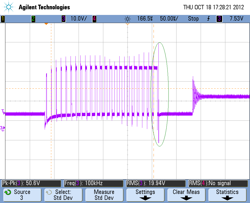
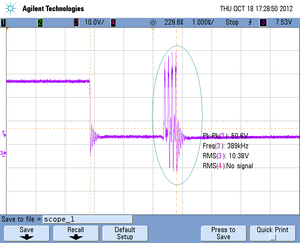
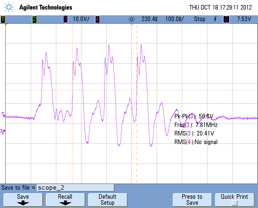
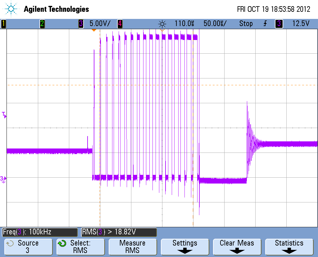
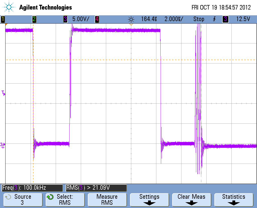
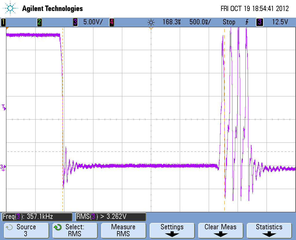
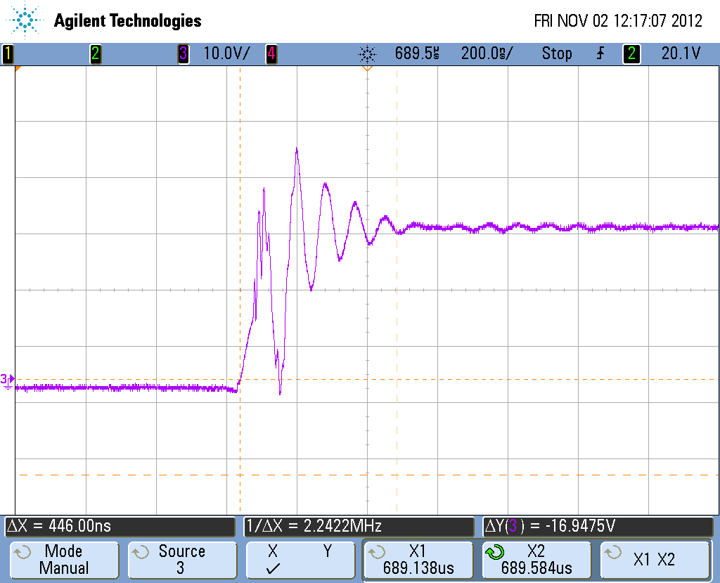
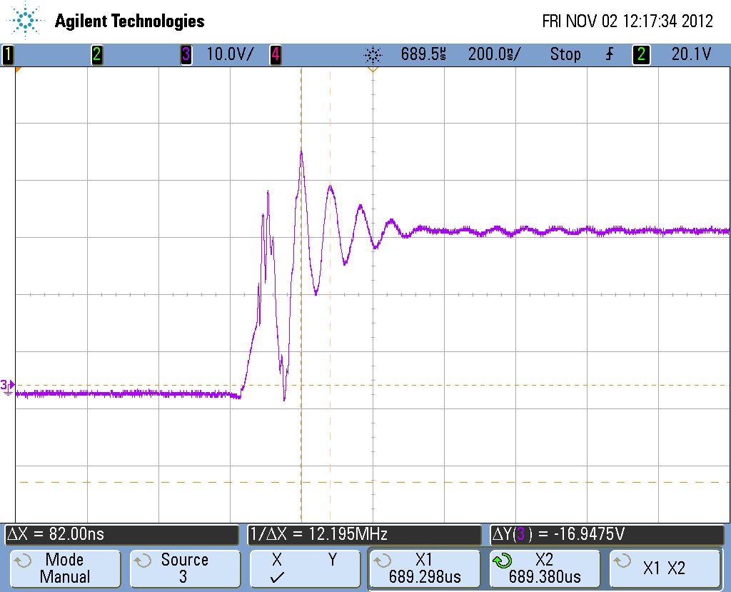
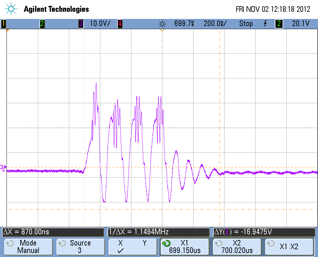
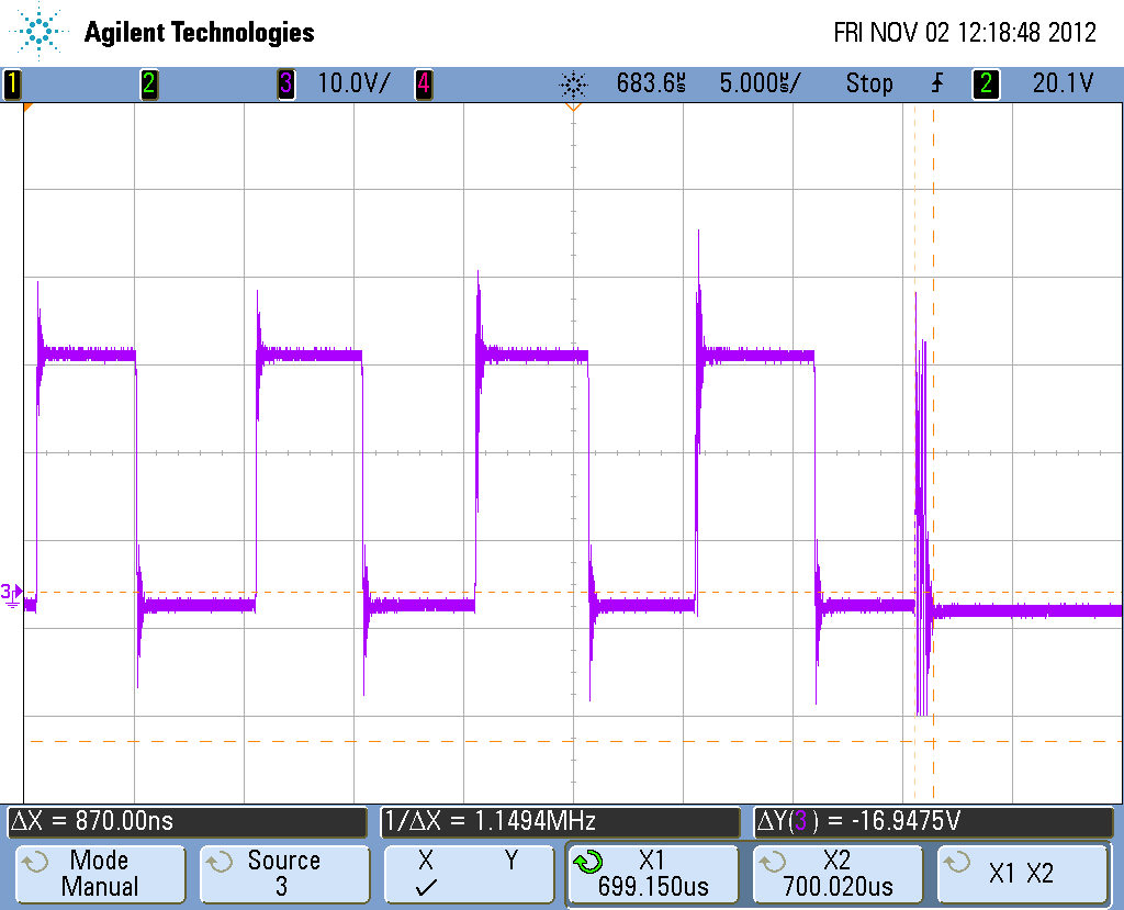
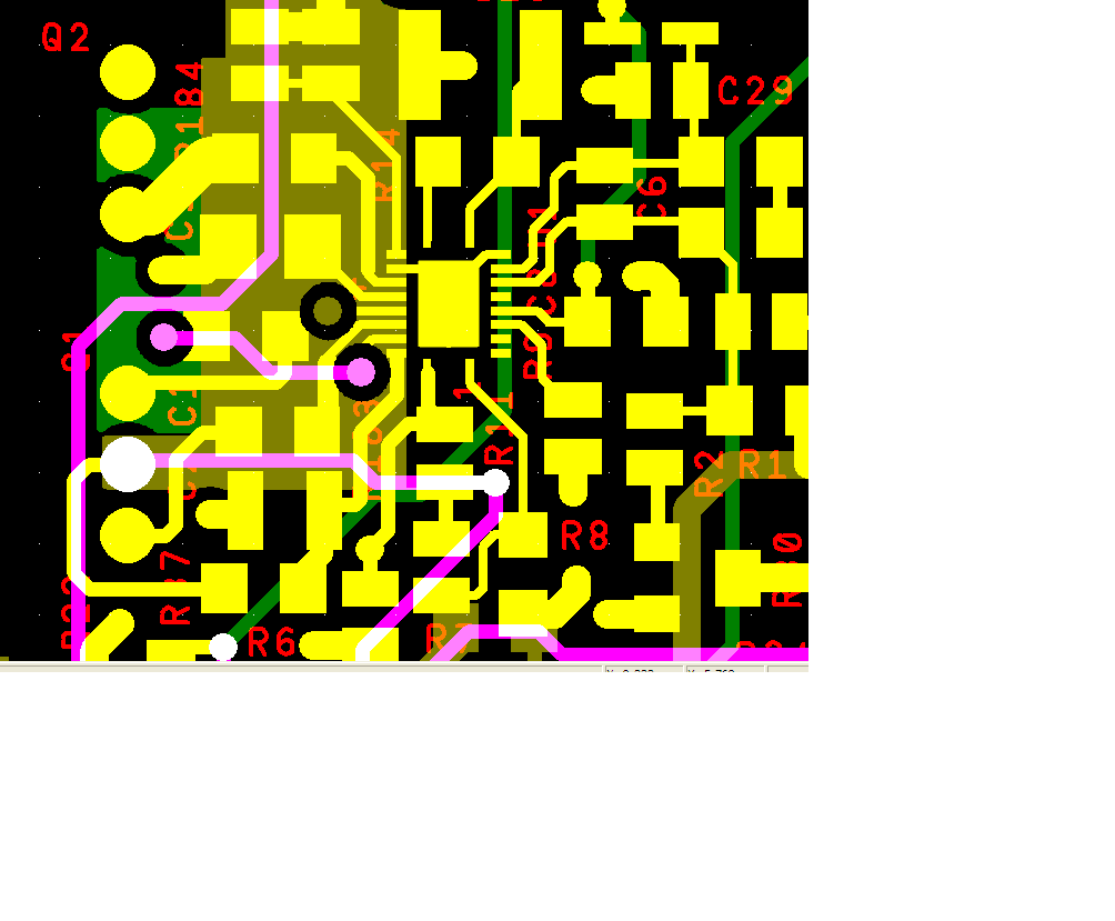
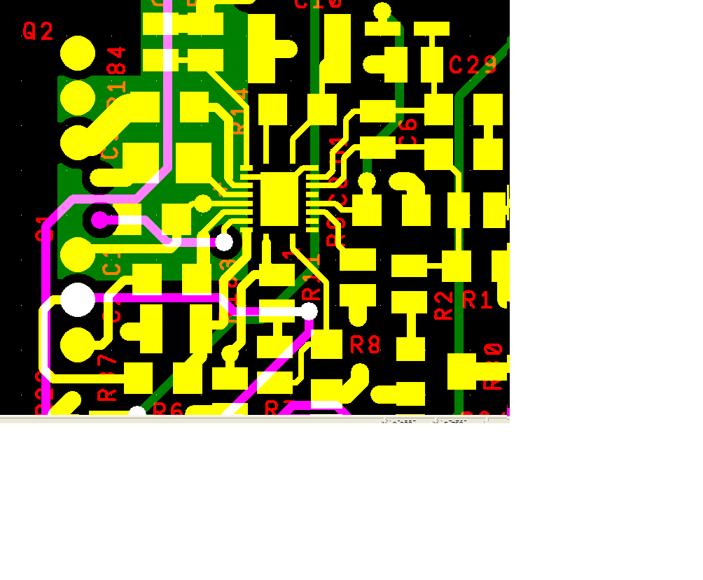
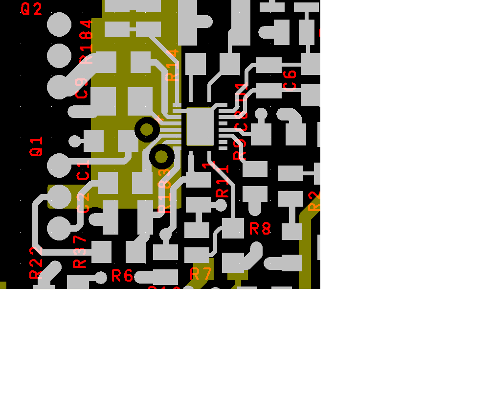
I am using TPS40170 in my buck converter. Input 18-32 V, Output - 15V, Max current - 4A. When I observed the SS capacitor, it is found that the voltage switches between 2.5V and 300mV, indicating that there could be some fault condition(Temperature, OCP and SCP), As I have not connected any load, OCP and SCP cannot happen. Even the device is found to be very cool which concludes that there is no over temperature fault. I have left out with, ringing, which causes the scp or ocp condition. I have noticed ringing on the high side gate pulse with a frequency of 8MHz which causes the device to shut down. The ringing occurs when the HIgh side mosfet, switches on, which in turn trigger SCP (as i believe)   The same ringing frequency is seen in boot capacitor also. I am using a boot cap value of 100nF. The MOSFET used was IRF540Z. We have used our own custom board. I have tried all known methods to avoid the condition like adding a series R to boot cap or changing the value of boot cap, addition of snubber circuit at the SW node etc...etc...Kindly anyone help to resolve the issue.

  • Hi Manu,

    You are correct it appears something is falsely triggering the SCP or OCP. Can you please post your schematic and layout?

    Regards,
    Anthony

  • Hello Anthony,

     Thanks for the response. I am attaching the schematic and layout. Also I am attaching the waveforms noticed on the HDRV pin. Kindly note that I have changed RT to have a switching frequency of 100KHz.. Note that the ringing is observed even with 300KHz switching frequency(as per the design in the schematic)

    4150.schematic.PDF

    5305.component_side.PDF

    6371.solder_side.PDF

  • Manu, thank you for the detailed information. Judging by the switching waveform you might be running into issues where the boot capacitor is running out of charge for driving the high-side FET. Is there a prebias voltage on the output during turn on? There appears to be one of about 8-9V. Have you or can you test startup with no voltage present?

  • Hi Anthony,

     Thanks for the reply and advice. I am attaching the waveforms with no prebias at the output. We don't have a prebias at the output. As I have not connected any load, the previous charge on the large output cap may be appearing as prebias in the earlier waveforms.

    I have tried by increasing the boot cap, but it didn't resolve the issue.

  • Hi All,

     Any update/suggestion on the above issue?

    Kindly help

  • Hi Manu,

    I apologize for the delay, I was out for a few days this week.

    A few more suggestions I have:

    -Can you show a few more waveforms in this setup, what does the output voltage and gate drive signals look like?
    -Have you double checked the loop stability? The TPS40k Type III stability tool in the product folder will work.
    -I haven't done any calculations but the 100uH inductance seems very large. How was this selected?
    -What happens if you replace the gate drive resistors R183 and R184 with 0 ohm? Also try changing R6 to 0 ohm.
    -I don't think this is a source of the issue but TRK should be connected to VDD if not used to help avoid noise from affecting the regulation of the output.
    -Do you have a layout which shows the copper as well? Make sure all guidelines in the datasheet are followed. I may also be interested in checking out your BOM.

    Regards,
    Anthony

  • Hi Anthony,

    Again thanks for your valuable suggestions. Please note my observations regarding the above topic

    1) I have checked the loop stability using the tool and its found to be OK, I have chosen  a phase margin of 65 deg. Also please note that the same gate oscillations were noticed in OPEN LOOP also.

    2) The 100uH was selected based on one of our earlier designs of power stage, but now I have changed to 33uH, then also there is no improvement, even I have changed the capacitor to 22uF (as given by TI ref design tool), but still the oscillations were observed. I have tried changing R183 and R184 to 0 Ohm and even shorted directly using a jumper to avoid the track in the PCB, the R6 is changed to 0 ohm. Also ENB pin was directly connected to VDD  (so that ENB will not get any noises from the main supply ) but no improvement is seen.

    3)  The TRK pin - With much difficulty we pulled this pin to VDD using a jumper, even this also didn't improve the condition.

    4)  We have taken care to follow all the guidelines mentioned in the datasheet during placement and routing

    I am attaching a few more wave forms

    1) VOUT waveform (noticed in the open loop condition)

    2) The waveform at SS pin (open loop)

    Kindly analyze and suggest any improvements if you have

    Regards,

    Manu Antony

  • Hi Manu,

    After looking at your layout again there may be some improvements here to help reduce the ringing during the turn on of the the high-side FET. Can you show a screenshot zoomed in on the rising edge of the last normal pulse seen? I'm curious how long the ringing lasts.

    Can you please post your layout again showing the copper areas and traces as well? I can't make a thorough judgement from only the placement.

    Thanks,
    Anthony

  • Hello Anthony,

    I am posting few more inputs as you have requested. The waveforms are captured with the circuit in open loop condition

    Attached below is the zoomed screen shot of rising edge of last normal pulse seen

    As you can notice in the below waveform the ringing lasted for around 870 nS

    I am attaching the layout with copper tracks, The layer details are given below

    Total we have 6 layers

    Top layer - Signal routing - Grey/Yellow color

    Second Layer - GND

    Third layer - Signal routing - dark green color

    Fourth layer - signal routing - violet color

    Fifth layer - GND

    bottom layer - signal routing - Olive green color

    1) All layers

    2) All layers excluding bottom side

    3) Top and bottom side layers

    Kindly suggest any other modification if required

    Thanks and reagrds,

    Manu Antony

  • Hi Manu,

    Took us a bit to get there but I believe the ringing on the rising edge on the last pulse is the main source of the issue. But first let me make sure of the measurement technique here. Was a short GND lead used to minimize the inductive coupling into the probe?

    You will want the largest peaks of the ringing to last about 55ns max. To do this you will want to include what you have already tried plus you may need to improve your layout. Make sure your RC snubber is optimized and use the bootstrap resistor to increase the turn on time of the high-side FET. Although I did ask you to try taking them off and am guessing they were not used in this measurement. I would also keep R6 at zero ohm as this has been known to affect the accuracy of the OCP/SCP trip point.

    Another improvement here will be with your layout. The placement of the input capacitors and the FETs is critical especially when leaded FETs are used. The parasitic inductance of the leads can greatly increase the ringing so the design is challenging with the TPS40170 because it uses Rdson sensing. You may also want to include more ceramic capacitance close to your FET. This should be connected as close as possible from the drain of Q1 to the source of Q2 to minimize parasitics in high frequency current switching path. Can you try placing a 1µF or 2.2µF ceramic here to see if it reduces the ringing?

    Some minor improvements in the trip point may also be seen by making some space to move your VDD and VIN capacitors next to the IC. You could do this by moving your PGOOD resistor further away to bring the VDD capacitor closer to the VDD pin and AGND pin. For the VIN capacitor you can move the UVLO resistors over. Are these two capacitors ceramics as recommended by the datasheet?

    Regards,
    Anthony

  • Dear Anthony,

     Thanks for your help and valuable suggestions. We have used short leaded probes.  But I am yet to come out of the problem. As you have indicated, the lead inductance of the MOSFETs and parasitic of the board may be adding fuel to the problem. I have tried almost all the possibly ways to make make the board work, but failed. Is there any way to bypass the SCP/OCP?

    Tried changing snubber elements, but they doesn't seems to have any affect on the ringing, the boot strapped resistors were changed many times, R6 is reduced to 0 ohm, tried placing ceramic capacitors closer to the high side mosfet. May be if I change the entire board layout, it may work. But as the process cycle time (PCB design, manufacture, assembly etc) is large and also there is a bit of risk that it may not work after changing the layout, I may opt for changing the design itself. Can you suggest any other proved simple voltage mode pwm controller and driver ICs which goes well with leaded mosfets. It need not have any type of current protection. May be the well old Unitode products are sufficient for our design.

    Thanks and regards,

    Manu