This thread has been locked.

If you have a related question, please click the "Ask a related question" button in the top right corner. The newly created question will be automatically linked to this question.

TPS40210 12V->180V efficiency problems

Other Parts Discussed in Thread: TPS40210, SWITCHERPRO

I've built a boost converter, 12V->180V, using TPS40210. I am trying to replace a design based on a MAX1771.

The new design works, and at a first glance behaves great: low ripple, no significant noise anywhere in the circuit, behaves nicely under load. Problem is, the efficiency is only 45% at 13 mA load! I expected to get at least to 75%, which is what the similar circuit using the Maxim part gets.

I expected to be able to get up to 85mA @ 180V from this circuit. The (shielded) 100uH inductor has a peak current of 2.4A (the inductor is MCSDRH125B series from Multicomp). The MOSFET is an IRFH5025, with RdsON=84mOhm, Qg=37nC, Qgs=8.3nC.

The losses seem to be incurred in the inductor, as this is the part that gets hot after a short time. Now, I'm puzzled, because I'm comparing this board to one just next to it: the other one is based on MAX1771, uses the same inductor and an IRF644, which has much worse parameters (RdsON=280mOhm, Qg=68nC, Qgs=11nC). And in spite of many problems (noise in the feedback circuit, ringing, etc) has no problems reaching 75% efficiency with the exact same load. The inductor doesn't even get warm. So why does it get hot on the TPS40210 board?

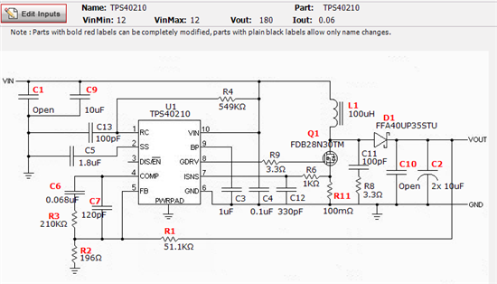
I am posting the relevant part of the schematic and the switcherpro output, which this design is based on (please ignore the double inductor, it is there only to provide pads/vias for both SMD and THT inductors). I can also post pictures of the PCB design and the assembled circuit itself.

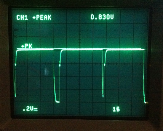
Also, I'm attaching a picture of the gate signal of the MOSFET, taken with a 10x probe. I find the duty cycle highly suspicious.

I've searched the forum for past replies to similar problems -- and in many cases it is suggested that Qgs of the MOSFET might be the problem. But if so, how does the MAX1771 manage to perform much better even with a much worse MOSFET?

Looking for help and advice from more experienced colleagues. Any hints appreciated!

  • Hi Jan,

    Looking at the gate drive screenshot makes me think it might be unstable. Can you modify up the SwitcherPro design to match your circuit to check the loop stability? Main components to change being the inductor, current sense resistor, output capacitor, fb resistors and compensation components.

    Regards,
    Anthony

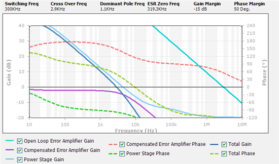
  • Ok, I did my best to try and exactly reproduce my components in SwitcherPro. This is the loop response graph I get:

    It seems that the choice of output capacitor (C10/C2) has a huge influence? That is not something I expected or knew about.

    In the meantime I also discovered that I mistakenly placed two 0R100 resistors in parallel as Rsense, instead of just one. The two resistors in my schematic are only to provide an easy way to build Rsense with smaller power rating parts. After removing one (which leaves Rsense as 0R100) the situation does not change. If anything, the inductor gets hot even faster.

  • Hi Jan,

    The output capacitor does have a big influence on the control loop. The output capacitor and the load current decide the Dominant Pole Frequency which is 1.1kHz in the SwitcherPro screenshot you gave. Based on this your compensation looks fine.

    You might be running into the maximum duty cycle limitation of the TPS40210 with this conversion ratio based on the minimum off time. Not including any efficiency losses for the real duty cycle the calculated off time is 222ns. If you assume 80% efficiency the off time drops to 178ns.

    One thing you cant try is to decrease the switching frequency from 300kHz to 50kHz to see if there is any improvement. This will increase the off-time. After doing this you will also need to decrease Rsense for the higher peak currents so you don't trip the ocp.

    Regards,
    Anthony

  • Thank you very much for the advice so far!

    The problem with my output capacitor is that I don't really have a lot of choice there. It has to be rated at 250V+, and most inexpensive ones don't even have ESR specified, which makes it difficult to model them precisely in SwitcherPro. I'm using one 4.7uF electrolytic and one 0.1uF X2 film capacitor on the output.

    Also, this is a design that (if successful) will be used by hobbyists to build power supplies for Nixie projects, so there will be part variation.

    In the meantime, having decided that I understand way too little from those graphs, I took the time to peruse some chapters from Marty Brown's "Practical Switching Power Supply Design" book. But armed with new knowledge I couldn't really see anything wrong with my compensation.

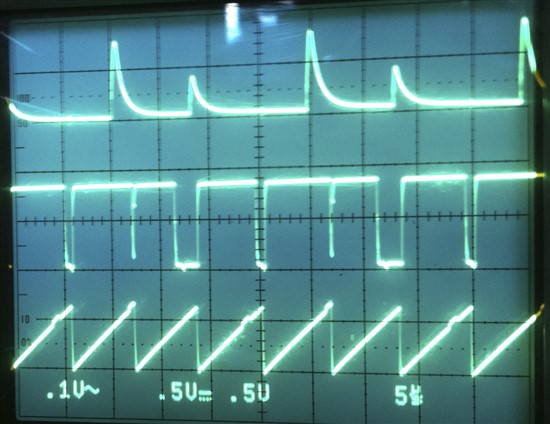
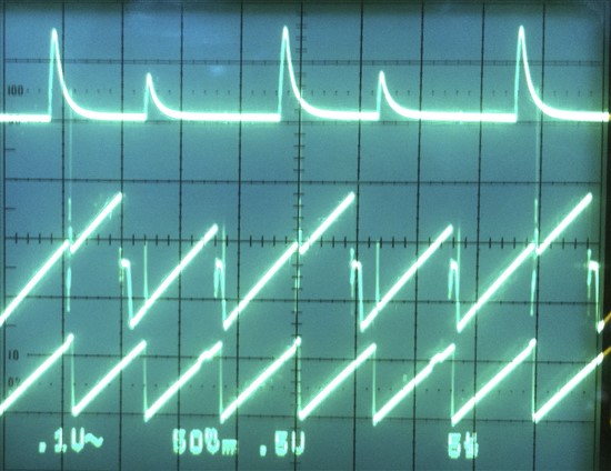
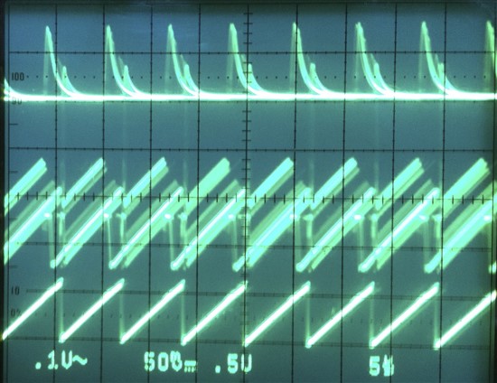
    Before I go for trial-and-error I would like to try to understand what's going on. I've attached some traces, perhaps these will immediately ring a bell? Sorry for the poor quality, but this *is* a hobby project, after all :-)

    My circuit is very sensitive to input voltage. I can get it to behave well if I turn the knob on my lab supply — there are certain areas where it works well, and others where even my scope traces become messy.

    This is the gate trace (middle). Top line is the output voltage, bottom is pin 1 of the TPS40210, this is what I use for triggering to get a stable trace.

    I don't know where the little ripple on the bottom trace comes from. It isn't present in my VCC and it isn't synchronized with anything I can see.


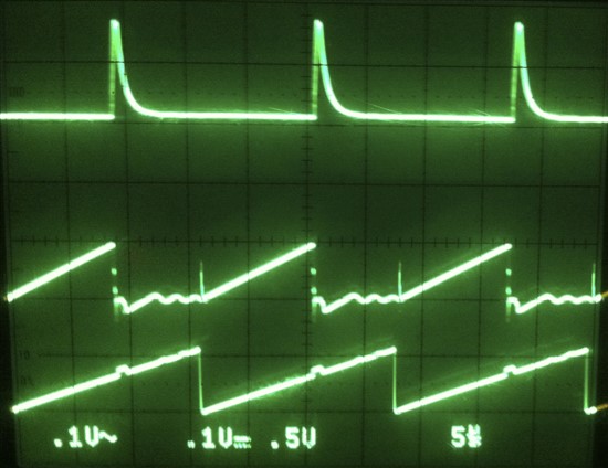
    This is a trace (middle) taken directly across Rsense (0R100 in my case):


    Top and bottom traces are the same as previously. Note that it goes negative (my zero line for the middle trace is at -1 division).

    And this is the same setup, but with the voltage turned slightly off the ideal 13.1V:


    Ok, I'll go try a much lower switching frequency now.

  • I'm glad to report that indeed decreasing the frequency seems to improve things a lot. I did lots of experimentation and the unstable behavior is related to duty cycle. I can provoke it at will by decreasing input voltage (which increases the duty cycle).

    I finally settled on 30kHz (1mOhm, 560pF), going lower did not improve things noticeably. At this frequency I have a stable circuit and I'm getting 75% efficiency, which while not exciting, is OK for my application.

    Unfortunately, I wasn't able to hit my goal of 60mA output current with 12V input voltage. If I load the circuit so that output current is 55mA, I need to take the input voltage to 15V, otherwise the duty cycle gets too high and the circuit is unstable. This is disappointing, as people get better results with MAX1771 (from just 9V): http://www.desmith.net/NMdS/Electronics/NixiePSU.html (higher currents, 85% efficiency, 9V operation) — and I am not sure what I can do to improve the situation in the TPS40210 circuit. I already use a much better FET.

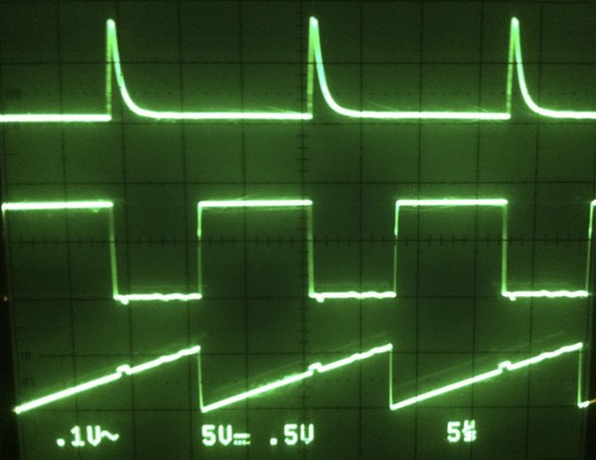
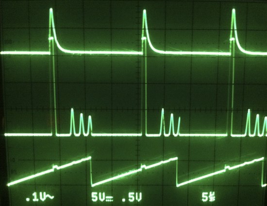
    And just for the reference, here are the current traces. Bottom: RC pin, top: output voltage, middle: Rsense.

    Bottom: RC pin, top: output voltage, middle: FET gate.

    Bottom: RC pin, top: output voltage, middle: FET drain.

  • Hi Jan,

    Good to see lowering the switching frequency did help. When operating near the limit every little bit will help your design to work. I would take care to minimize all losses in the circuit to reduce the effective duty cycle and to look over the layout to see if anything can be improved. Some of the most important connections and signals will be those related to the gate drive of the external FET.

    I also want to comment on the final 30kHz switching frequency. This is out of the spec range so not everything will be guaranteed by the datasheet. But in your case because you say it is hobby project it is likely ok. I'm assuming you aren't planning to go into mass production with your design.

    The MAX1771 does have a couple things allowing it to work in this application. The control method looks to be more of a hysteric control. When operating near the minimum on time the switching frequency changes. The disadvantage here is the switching frequency will not be predictable. Also with switching frequency decreasing there will be more ripple on the output. Lastly its lower operating current is helping the efficiency at the lower load current.

    Regards,
    Anthony

  • This is the layout I have (any feedback is appreciated). I don't see how I can make the gate trace much shorter. My main goal in this layout was to keep the high-current loops away from the low-voltage part of the feedback circuit.

    As for mass production, no, this is a hobby project, but it isn't a one-off either -- I do expect people will build this design, which is why I'm spending quite a bit of time on it. I will test the behavior at various frequencies again, then.

    Many thanks for your help on this so far.

  • Hi Jan,

    Another suggestion I have is to replace the gate drive resistor R9 with a 0 ohm resistor. Reducing this can increase the slew rate of the gate drive signal to help turn on the FET as fast as possible for operating at the higher duty cycles.

    Looking over the layout it looks good. Ideally I would try to have the ground of the output capacitor C11 right next to the ground of the current sense resistors while keeping the VOUT side of the output capacitor close to the diode. But with the high voltage design you become limited by the components you can select and the snubber is in the way.

    I didn't look closely at it before but it looks like C8, C2, D2, and D3 are used to create a charge pump? What is this used for?

    Anthony

  • Ok, so the circuit's efficiency isn't bad at all. It turns out that the numbers displayed on my Chinese power supply have little to do with reality, voltage sags under load and the built-in voltmeter lies. The joys of hobby equipment :-) Now I carefully verify my Vin when doing any measurements.

    I also forgot that I should re-calculate the Visns RC filter for these lower frequencies, so now I'm using 1.8nF for the cap there.

    After performing a bunch of experiments: I am getting 85-86% efficiency at frequencies ranging from 30kHz to 50kHz. I consider this to be a very good result for this boost circuit. Going higher, efficiency starts to drop (81% at 76kHz). So, I'd be perfectly happy with running the TPS40210 at 50kHz. I've measured 86% efficiency at this frequency, with a 54.5mA load.

    I should rephrase my problem/question now: my problem is not the efficiency, but minimum Vin. All my measurements were taken at 13V Vin. The circuit has problems with lower input voltages: as I approach 12V I see some sort of instability, and as I lower the voltage even further, the TPS40210 shuts down (SS cap gets discharged). As for the instability, it looks like TPS40210 starts skipping pulses — is that possible?

    My question is: why would that happen and what can I do about it?

    I did lots of experiments trying to figure out the reason for the limitation. Even tried another inductor, a huge 5A-rated monster. Here's what I know so far:

    * The lower the frequency, the lower the minimum voltage. At 30kHz I can go down to about 11.4V before shutdown. At 50kHz the minimum is around 12.4V.

    * Removing Rg (as you suggested) has no measurable effect. The gate waveform looks as pretty as it did before, and the FET doesn't even get hot. I think my switching losses are small. I will leave it out, because of the large gate charge of this FET. The gate drive (both switch-on and switch-off) really looks vertical on my scope in comparison to the duty cycle.

    * Adding another 4.7uF/250V cap straight from the diode to the ground of the current sense resistors only makes Vout ripple smaller. No other change.

    * Adding 100uF on Vin right next to the inductor (in case it couldn't ramp up current fast enough) doesn't change anything.

    * It doesn't seem like overcurrent protection kicking in? My peak Visns is 120mV on a 50mOhm Rsns. That's 2.4A. Visns does not exceed the Visns(OC) 150mV value from the datasheet.

    * The maximum duty cycle I'm seeing is 94%. I could not find a limitation of the duty cycle in the TPS40210 datasheet.

    Here's what it looks like on the scope. There are just two traces, voltage across Rsns and the RC pin. The three captures are taken as I turn the voltage dial slowly down. The duty cycle increases. Now, if the next cycle starts when Rsns is slightly negative, I get instability. The middle capture is the last stable point, as I turn the voltage lower and enter the largest negative trough, the controller shuts down. You can see the instable behavior in the third capture.

    I verified that the signal past the ISNS RC filter looks nice and clean, no negative potential there.

    So, what can I do to make this design work down to (say) 11V? That should still be around 94% duty cycle -- high, but workable?

    As for C8, C2, D2, and D3, well spotted -- this is a voltage doubler, to produce >400V for dekatrons. It's optional and doesn't really influence results if left unloaded. I actually left this part unpopulated on the board I'm working with now.

  • Hi Jan,

    Glad to see there has been some progress. I have come to never trust the voltage meter on power supplies :).

    Figure 2 gives some idea of the duty cycle limitations when using the TPS40210. The max duty cycle is determined by the minimum off time of 200ns. With 94% duty cycle the off time is about 1.2µs. The 200ns off time gives a theoretical max duty cycle of 99% with 50kHz switching frequency.

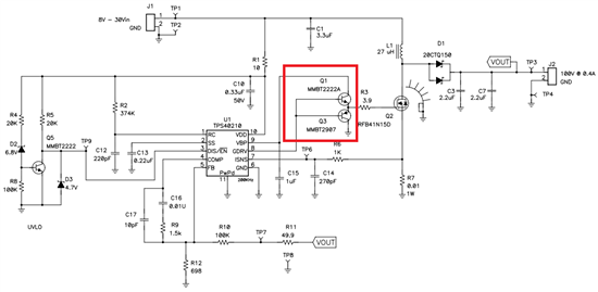
    What does the gate drive waveform look like as you approach instability? Another thing to try is add a transistor pair to boost and buffer the gate drive signal to the FET. Example in the picture below.

    Regards,
    Anthony

  • Anthony,

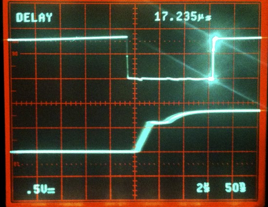
    Here's what my gate drive looks like. The bottom trace is a magnified part of the top one. As you can see, it takes about 100ns for the voltage to ramp up. That's with a 10x probe loading the gate.


    Are you sure I should try a gate driver circuit? It isn't easy to prototype, so I'd rather not, unless we're certain this is the right direction. The gate drive looks reasonable to me.

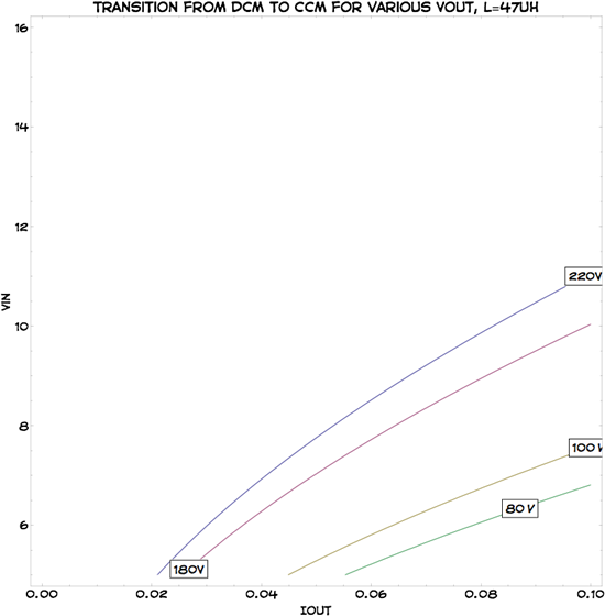
    I've done some thinking and looked at the triple screenshot I posted last time. I think my stability problems begin as the circuit transitions from DCM to CCM. I also took the liberty of doing a quick plot of the transition boundaries in my circuit, for various values of L in uH (this is based on the simplified equation (4) from page 12 of the datasheet):

    I'm testing the circuit with 53.5mA load, so it looks to me that I'm hitting the DCM/CCM boundary right around 11V, which is consistent with what I'm seeing.

    Given the high step-up and the wide range of output current, I don't think I can avoid the DCM/CCM transition.

    Now, I can't really show you how the traces "look" like when the circuit is unstable, because I can't really see them with my analog scope. It looks as if the peak voltages remain the same all over the circuit, but the duty cycle alternates between multiple values. No matter how I try, I can't get a stable trace.

    Isn't this related to sub-harmonic instability described on pages 15/16 of the datasheet? "alternating long and short pulses from the pulse width modulator" would be consistent with what I'm seeing (or not seeing) on the scope. Problem is, much as I try, I can't understand that section (BTW, Acs isn't defined anywhere, and m2 is defined, but not used). It also doesn't help that Risns(max) for my circuit is about 6mOhms, which isn't practical.

  • Jan,

    Good thinking and this is a very useful plot.

    From your description I think you're right with the subharmonic instability in CCM if your RSENSE is too large. I had not gone through these calculations to check your maximum value of RSENSE previously. Also when I looked at your 3 images to me it looked like you were at the DCM/CCM boundary too so it makes sense.

    To get around this is it ok for your design to operate in DCM the whole way? If so can you try reducing the inductance to see if you can get more output current? This will force you to stay in DCM and here you will completely avoid issues with subharmonic instability. When operating in DCM the current feedback path does influence the control loop. But you will need to make sure your OCP level is high enough to accommodate the higher peak current.

    Alternatively if you need to use 100uH and you want CCM you can try to reduce your current sense resistor further or divide the current sense signal down as suggested on page 16 of the datasheet. But this will also increase your peak current limit level.

    Lastly Acs is up in the electrical specifications table on page 4. This is the gain of the current sense amplifier. Sub-harmonic instability is something inherent to current mode control with duty cycles greater than 50%. A compensating ramp with a down slope (m2) must be added to the current ramp before it goes to the PWM logic to avoid instability. There are quite a few articles on it. Let me know where you're confused and I might be able to help you understand if you're interested.

    Regards,
    Anthony

  • Thanks! I intend to try both approaches:

    a) A smaller inductor. Operating in DCM is not a problem at all. But another quick plot shows that in order to support the maximum of 220V (which I'd like to be able to get to), I'd need to go down to 47uH. At 68uH I can't guarantee DCM operation at 11V Vin and 60mA/220V output. I haven't done the calculations yet, but I'm worried about peak currents.

    b) I'd really like to understand and implement slope compensation, but I don't feel comfortable taking up your time for something I can read myself. Thing is, much as I try to understand it, the section on subharmonic instability in the datasheet still does not make much sense to me. The referenced SLUA101 does explain the *problem* very well, but doesn't get me any closer to a solution. And most literature available online either explains the problem, or explains how to build slope compensation from a feedback or oscillator signal, which is not what I should be doing with the TPS40210.

    From what I understood, the TPS40210 has internal slope compensation. This means that my job as a designer is to provide a properly scaled signal at the ISNS pin, so that after passing through the current sense amplifier it "matches" the slope compensation signal generated inside from the oscillator. The current sense amplifier has a gain of roughly 6. Now, what I can't grasp is why the voltage compensating ramp slope is discussed if I have no influence over it. I guess I'd expect a "desired peak voltage for the ISNS signal", so that I can use a resistor divider to scale whatever I get from my (overly large) Risns. The datasheet hints at this kind of solution (last sentence in the section), but that hint is not enough for me :-(

    Am I way off? Please feel free to just point me to additional reading or just ignore this part.

  • Hi Jan,

    All this information is great. You've really helped to analyze using the TPS40210 in an application like this. Unless I've done my math incorrectly, with a 47µH inductor the peak current is only about 3.75A. I've attached the excel with my calculations with the below link.

    1172.TPS40210 220V Boost.xlsx

    Your understanding in b looks correct. The slope compensation is fixed and you have no influence. This equation is mostly to ensure the slope compensation is sufficient for the sense resistor selected in your design. It is discussed to help give some understanding of why this limitation is placed on the sense resistor. The slope of the actual internal ramp is given by Equation 8.

    Best Regards,
    Anthony

  • I redid the calculations and 68µH should leave enough margin to stay in DCM. Verified experimentally -- things work just fine with both 47µH and 68µH inductors. No unstable behavior anywhere in DCM, though I still have to build a circuit to test the transient response.

    Anthony Fagnani said:

    Your understanding in b looks correct. The slope compensation is fixed and you have no influence. This equation is mostly to ensure the slope compensation is sufficient for the sense resistor selected in your design. It is discussed to help give some understanding of why this limitation is placed on the sense resistor. The slope of the actual internal ramp is given by Equation 8.

    Ok. So my sense resistor is 50mΩ. The maximum calculated value to avoid instability is 3mΩ. Two questions:

    1. Am I right in thinking that by using the maximum acceptable value I basically give up overcurrent protection, and there is nothing that can be done about it?

    2. Instead of using a smaller Rsense, can I add a resistor across C12, thus forming a divider which would scale Vsense down?

  • Hi Jan,

    Good to see the lower inductor values worked well.

    1. Am I right in thinking that by using the maximum acceptable value I basically give up overcurrent protection, and there is nothing that can be done about it?

    Correct if you were to use 3mΩ the over current protection limit will be a very high current and won't provide much protection. However, when planning to operate in DCM for all conditions you do not have to follow this equation. When operating in DCM the slope compensation has no impact on the control loop. In this case the control loop operates more like voltage mode control. Instead the resistor can be set for over current protection only. But supply will most likely be unstable if it begins operating in CCM.

    2. Instead of using a smaller Rsense, can I add a resistor across C12, thus forming a divider which would scale Vsense down?

    Yes this works but will be equivalent to using a smaller resistance Rsense.

    Best Regards,
    Anthony