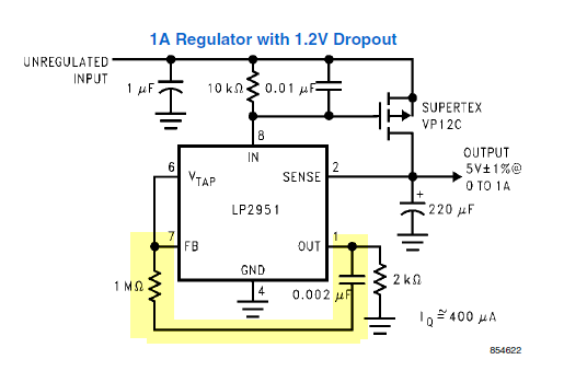
in the datasheet of lp2951
in typical applications,1A regulator with 1.2V dropout,
how they have chosen 0.002 uf between fb and out ?

-
Ask a related question
What is a related question?A related question is a question created from another question. When the related question is created, it will be automatically linked to the original question.