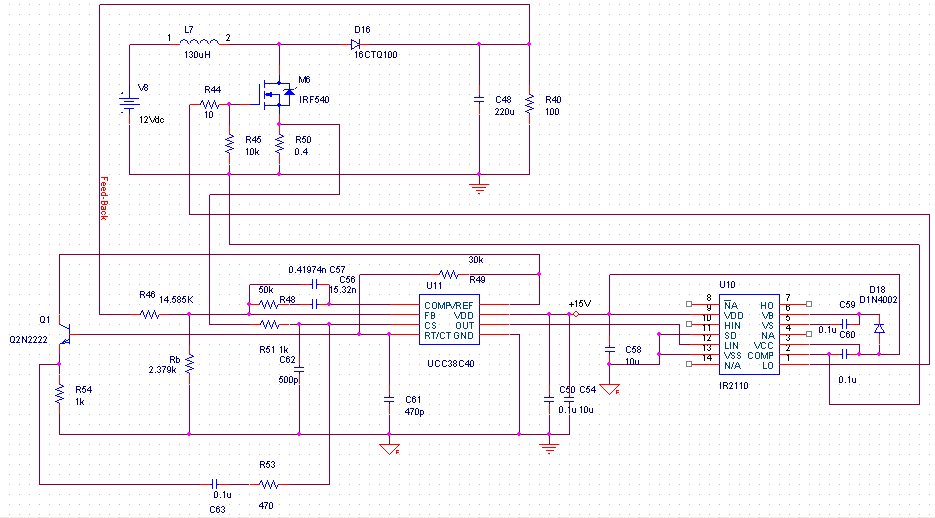
I design a boost converter using UCC38C40 as control chip, the parameters are, input voltage 12 V, output adjusted to 48 V and should work in CCM. I find some problems with output PWM duty cyle, it would not go to steady state even though output is stable.
The following are some waveform of circuit,
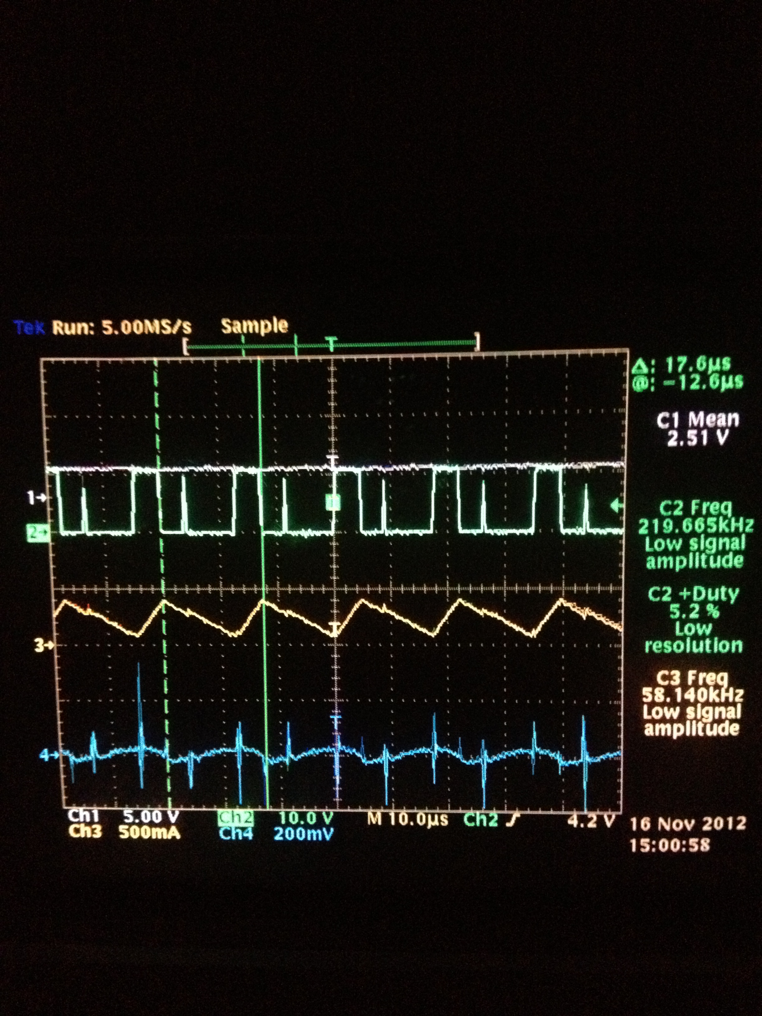
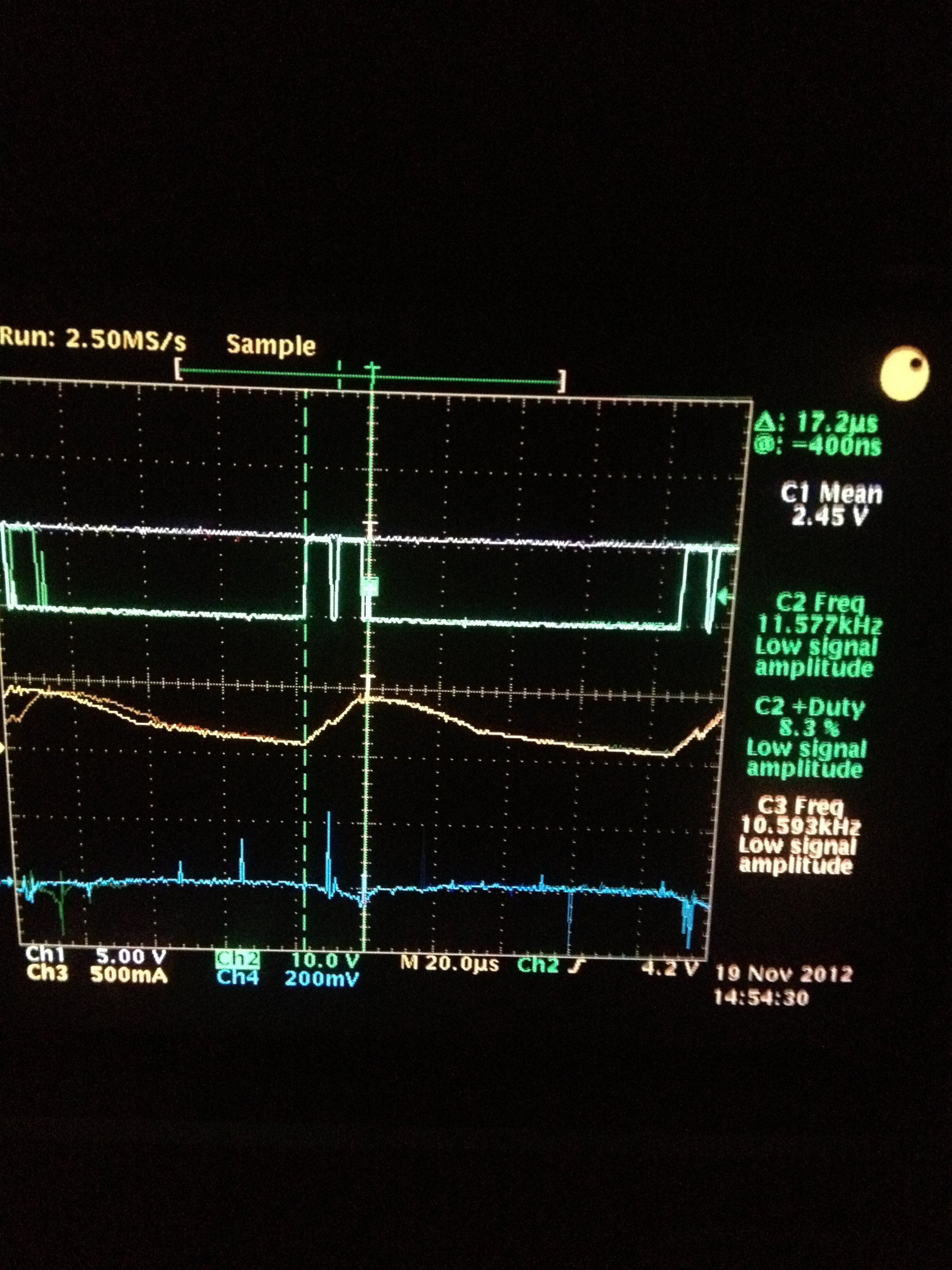
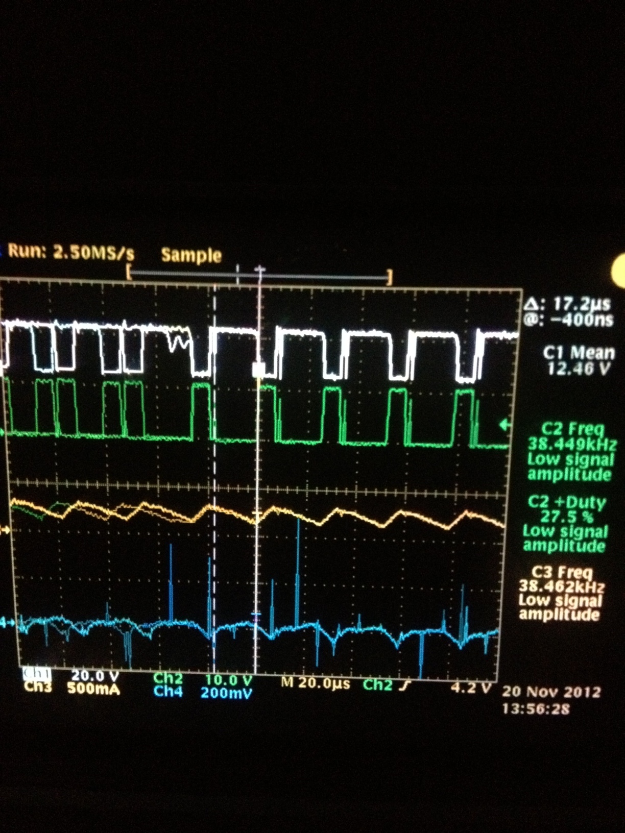
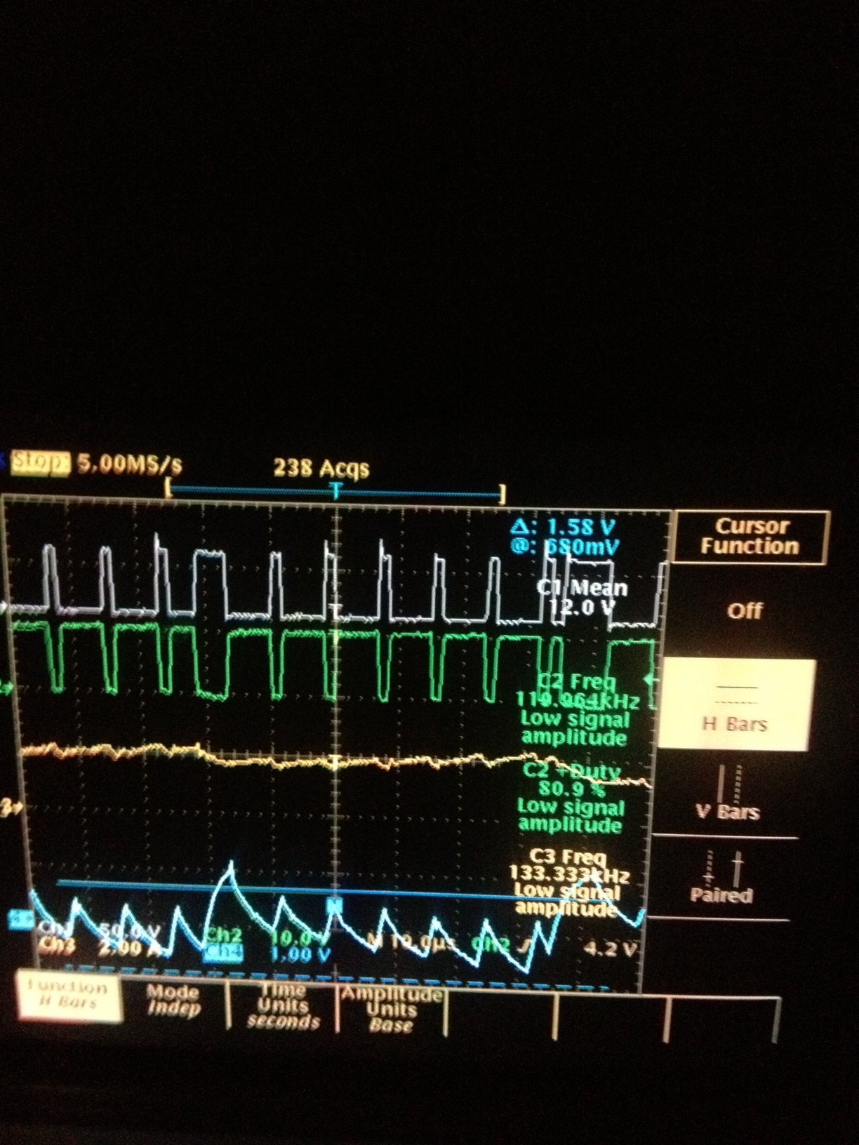
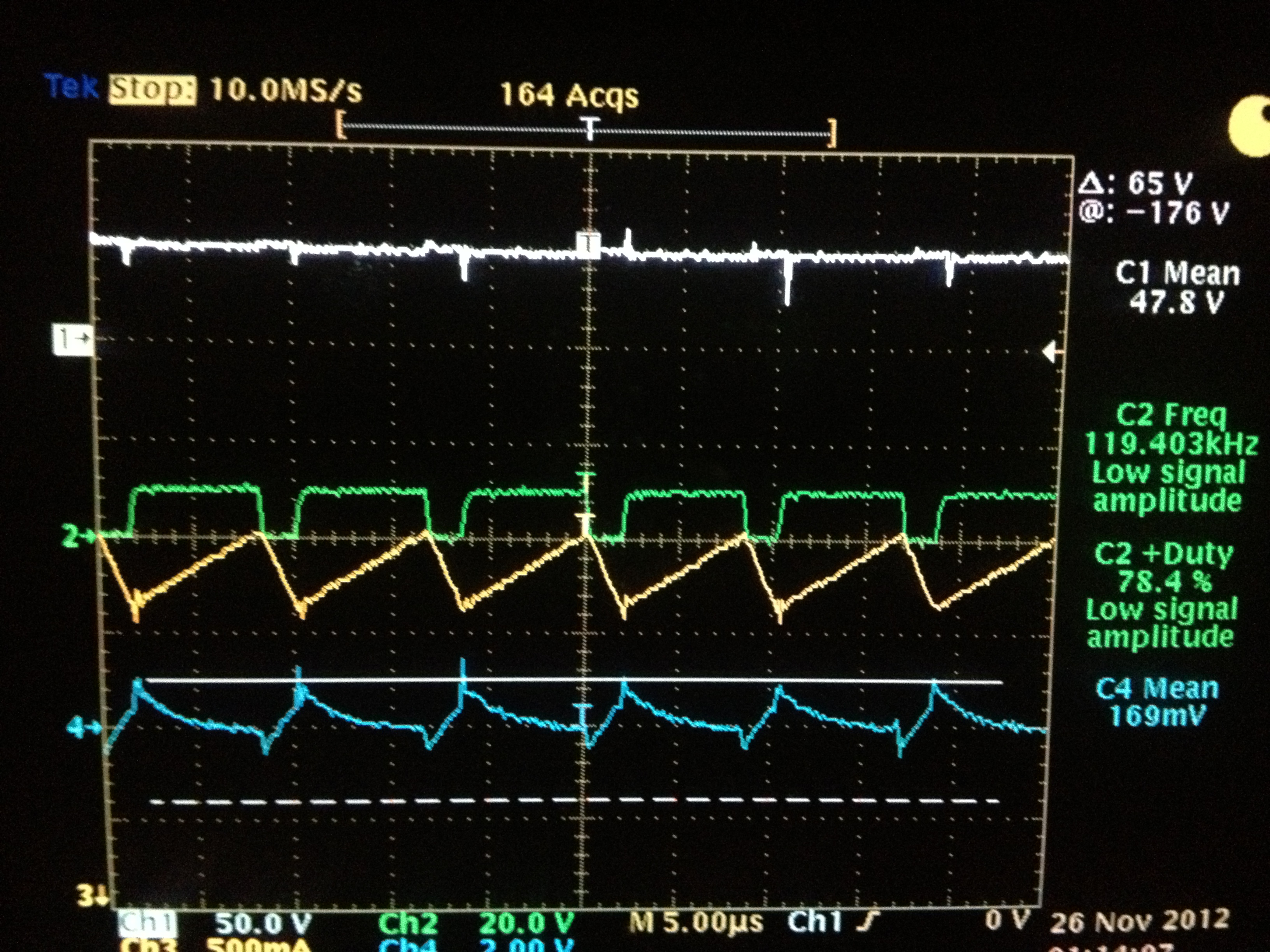
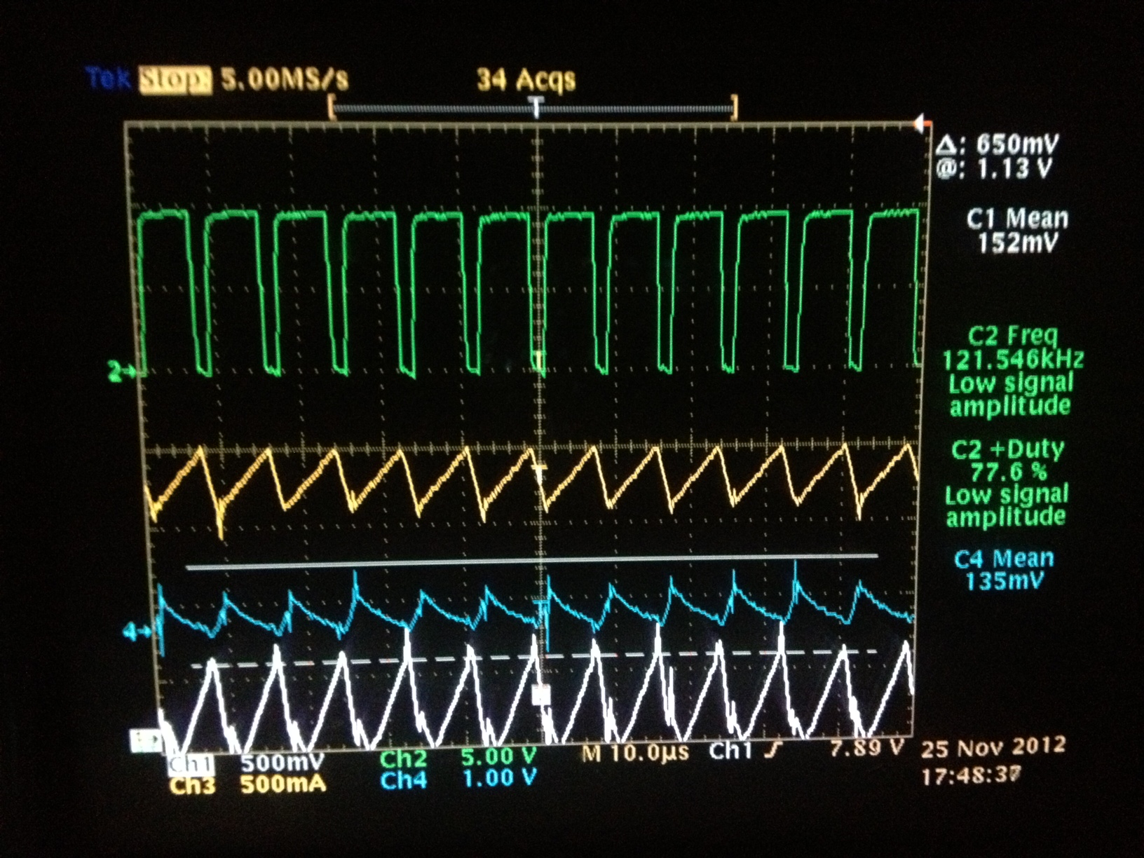
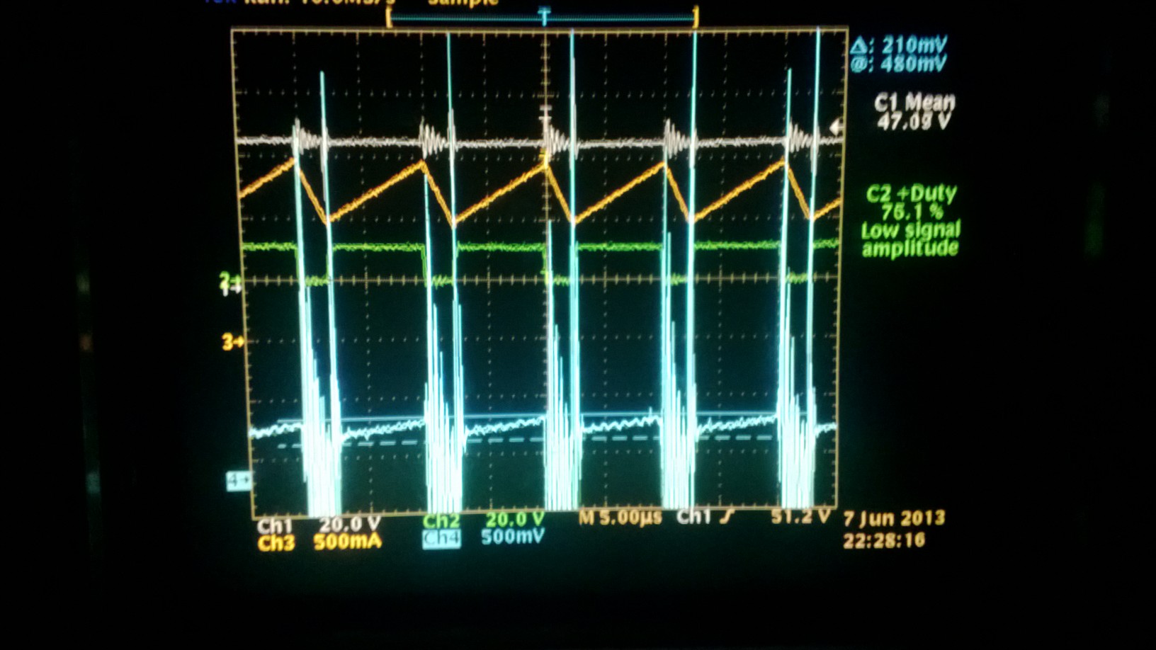
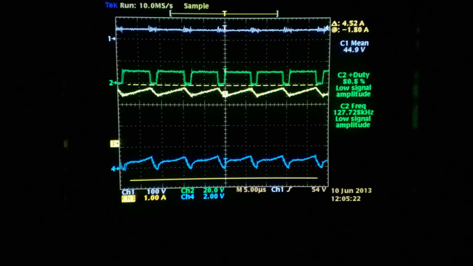
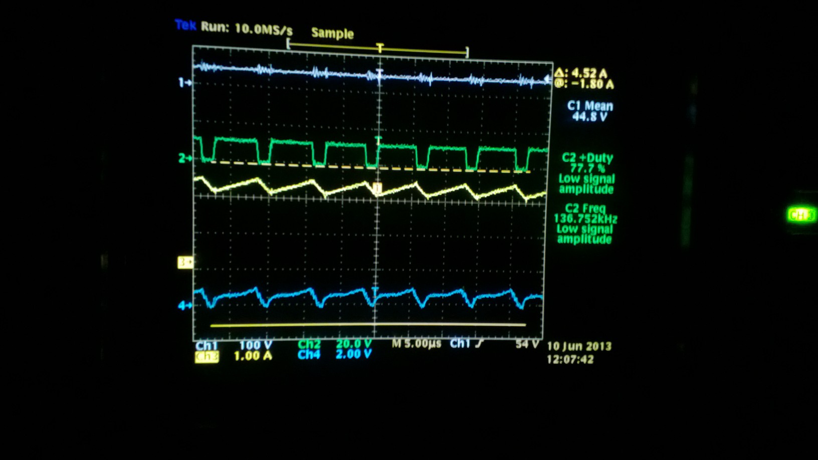
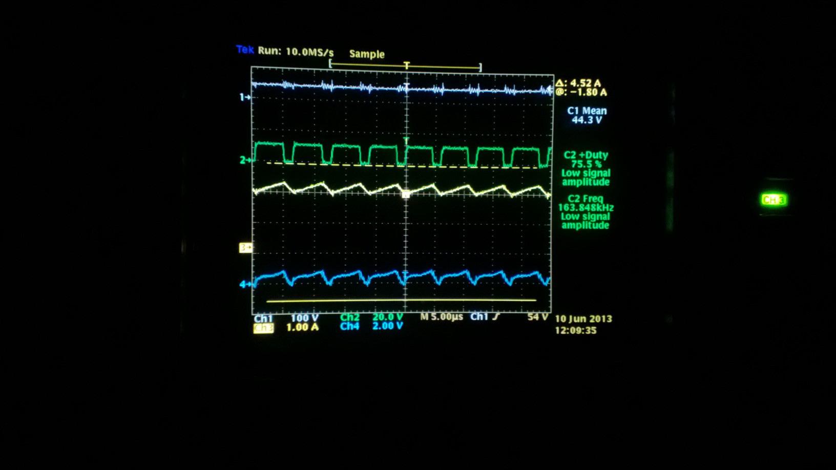
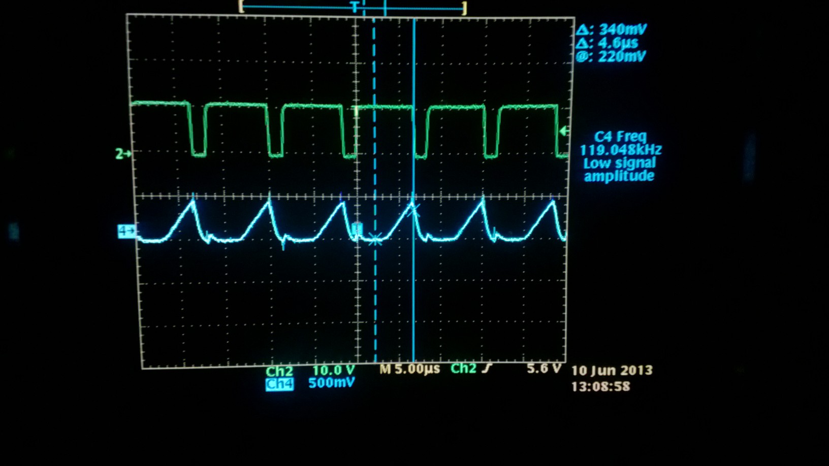
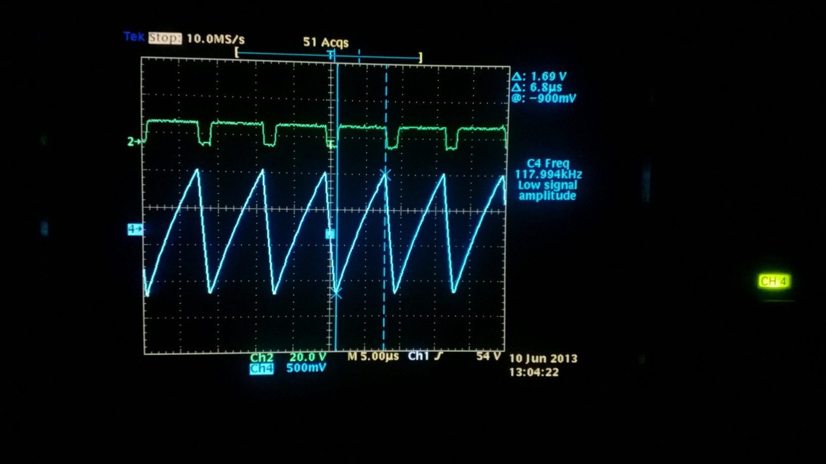
C1 white line is voltage on pin 1(FB), C2 green line is waveform of output PWM. C3 is input current. C4 is voltage on pin 3(current sense).
The output voltage is adjusted around 17 V. Ouput PWM duty cycle should be around 30%.When I test it in open loop, the control chip works at 116K Hz frequency.
The data in the image above is collected when circuit works in closed loop. The problem is that output PWM composed a wide pulse about 4.8 us(about 55.81% duty cycle based on 116K Hz) and a spike with same magnitude of pulse. I believe this spike is the initial of a sequence PWM.
I am wondering why can't PWM output be 30% duty cycle for each periode?
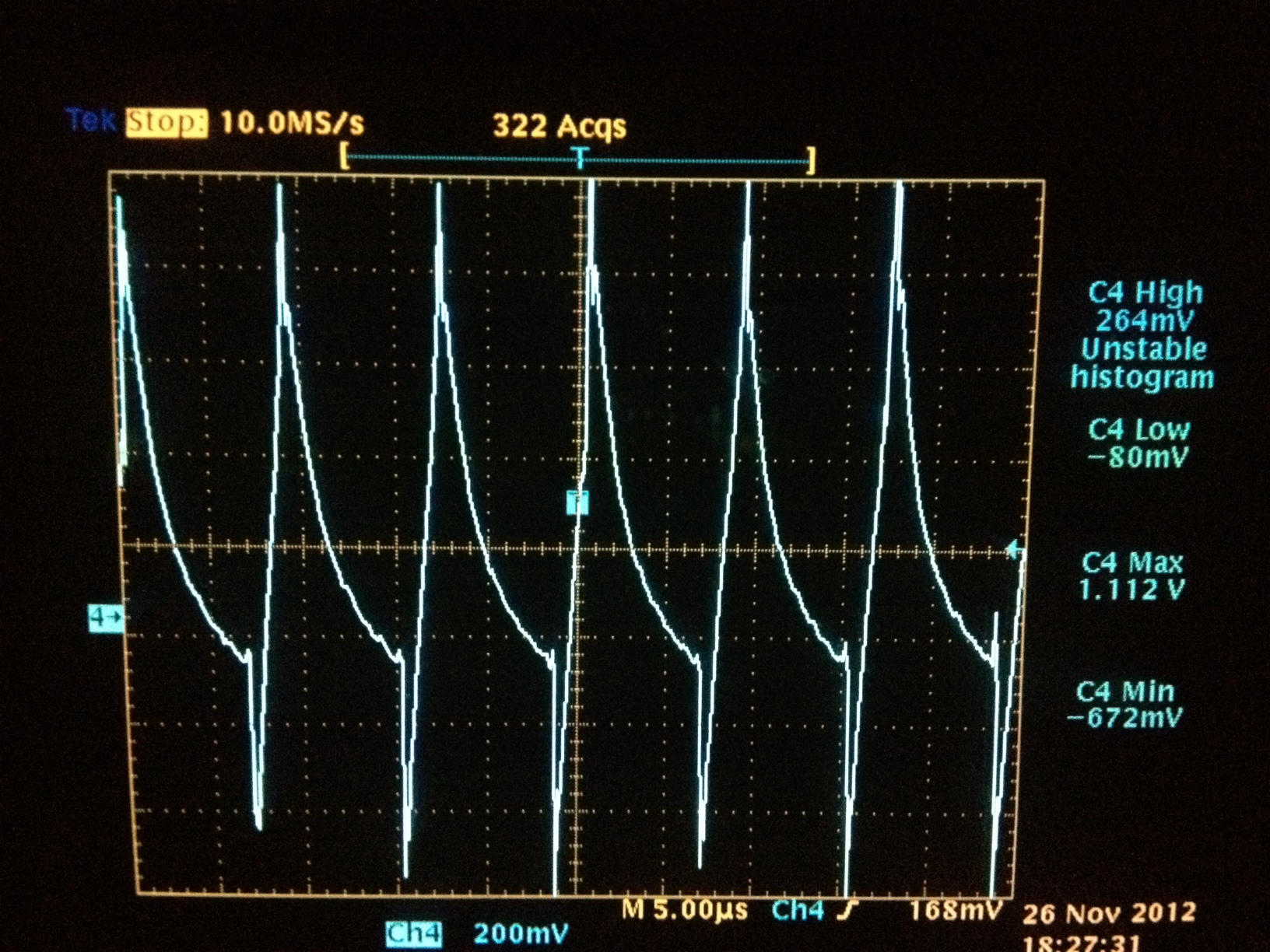
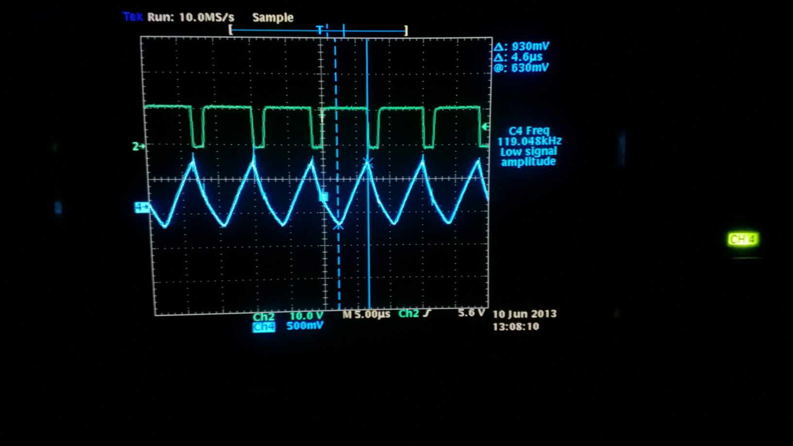
The bottom line (blue) is the voltage of current sense? Why it does not follow the ramp of input current which is in yellow in above image?
The following is circuit schematic
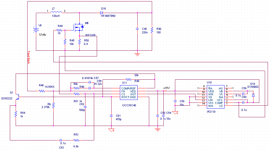
The input inductor is 130uH, it is my mistake that I don't correct it in schematic.
He, Siyu