This thread has been locked.

If you have a related question, please click the "Ask a related question" button in the top right corner. The newly created question will be automatically linked to this question.

LM3488 design out of spec at low temp.

Other Parts Discussed in Thread: LM3488, LM3478, LM3481

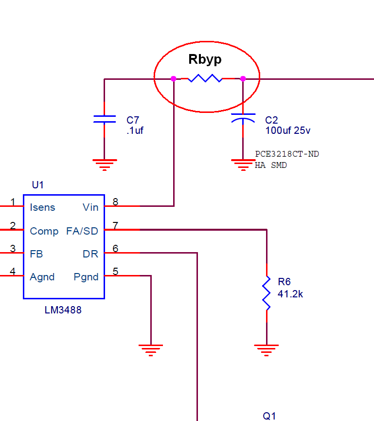
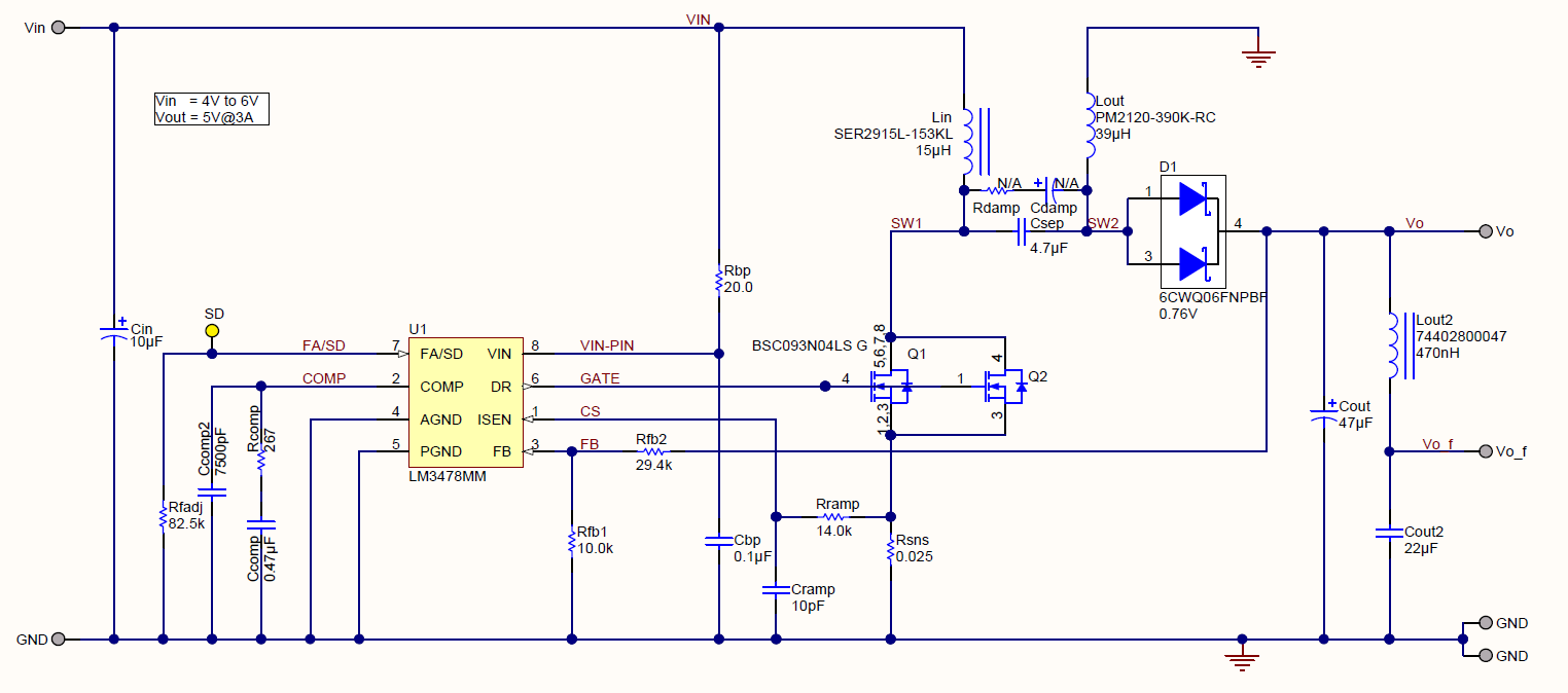
I have an LM3488 SPEC design that will not work correctly below apx. 32F.  It is rated to -40F.  I have re-evaluated the design with WEBench, and it still appears that the internal referance is drifting.  Normal load is 1.25A normal Vout is 12.5v, input is 9 to 15v. 

1948-902-00010r03.pdf
  • Hello Darell,

    could you please be more specific when you say the SEPIC converter will not work?

    Do you mean it just stops switching and then it restarts when the temperature is higher? is there a bad output regulation?

    just to be clear 32F therefore you mean 0C.

    Regards,

    Giuseppe

  • In the previous post I made on this problem, which has now been moved to this post(why?), I posted scope pictures of what was happening.  I will try and explain it.  Sweeping the ambient temperature and monitoring the drain of the FET you can see the device becoming more discontinuous as the temperature gets lower.  Like it is trying to regulate at a lower V point.  Once the temperature gets low enough the output V starts to drop as one would expect due to being discontinuous.  This looks more like the devices internal references are drifting and regulating at a lower voltage point.  If I try and start the unit under nominal load below about 32F, it will start running but the output V will be reduced.  The colder it is the greater this effect seems to be.  Yet If I start it with a greatly reduced load or no load it will come up with close to the normal voltage point but sage when a load is applied.  This leads me to believe the internal reference for the current sense is at fault.  I designed this for a customer that wants to use this in an automotive application and needs at least -20F operating range.  If I can not get an answer on this soon I will have to abandon this design , maybe I will look at Linear's stuff.

    I have went back and re-designed this useing TI's WEBench and found that I can improve this problem , but NOT cure it.  Is this desgn faultly or is there a silicon problem?

    Darrell

  • Hello Darell,

    unfortunately I never have met this problem with the LM3488.

    I will go ahead and review the schematic.

    Meanwhile could you please post your scopeshots showing the problem, also it would be very helpful to take a look at the PCB layout.

    Anyway my suggestion is to use the LM3481 which is an improved version of the LM3478/88.

    Regards,

    Giuseppe

  • Darell,

    does this problem occur with any input voltage?

    Also, I encourage you to use the LM3481

    Regards,

    Giuseppe

  • Giuseppe:

    Yes the problem exist under all operating conditions.

    Darrell

  • Hello Darell,

    we built your schematic on one of our built it boards and the circuit works fine.

    I took a look at your schematic and layout and I have some suggestions:

    1. make sure the power supply has enough current capabilty.

    2. Please introduce a 100 ohm bypass resistor like in the following image:

    3.The most important layout rule is to keep the AC current loops as small as possible. In a SEPIC regulator the primary switching loop consists of the output capacitor, diode, SEPIC capacitor, MOSFET and sensing resistor. Minimizing the area of this loop reduces the stray inductances and minimizes noise and possible erratic operation. On your layout i can see that the switching current goes from the top layer to the bottom layer throug vias and that's a very bad practice. I suggest you to put all the power component on one layer and make a tight AC current loop.

    4.The current sensing circuit in current mode devices can be easily effected by switching noise. This noise can cause duty cycle jitter which leads to increased spectral noise. The sensing resistor should be connected to the ISEN pin with a separate trace made as short as possible. Route this trace away from the inductor and the switch node. For the voltage loop, keep the feedback resistors close to the IC and run a trace as close as possible to the positive side of the output capacitor. As with the ISEN line, the FB line should be routed away from the inductor and the switch node. These measures minimize the length of high impedance lines and reduce noise pickup.

    5.A ground plane in the printed circuit board is recommended as a means to connect the quiet end (input voltage ground side) of the input filter capacitor to the output filter capacitors and the PGND pin of the controller. Connect all the low power ground connections directly to the regulator AGND. Connect the AGND and PGND pins together through a copper area covering the entire underside of the device. Place several vias in this underside copper area to ground plane. If a via is needed to connect the sensing resistor to the ISEN pin, then place that via in the inner side of the sensing resistor such that no current flow occurs. Place several vias from the ground side of the output capacitor(s) to ground place, that will minimize the path for AC current. The PGND and AGND pins have to be connected to the same ground very close to the IC. To avoid ground loop currents attach all the grounds of the system only at one point. A general rule of thumb is to maximize the low impedance area (VIN,VOUT, GND).

    6. Use thicker traces for the gate signal from the DR pin to the gate of the MOSFET.

    Like I previously wrote the circuit works well on bench and we can eventually ship out the board. Anyway i really suggest you to use the LM3481 instead of the LM3488 and to use webench for design a proper schematic.

    Please let me know if you need any further help.

    Regards,

    Giuseppe

  • Thank you for the reply.  I assume you did your testing at low temperatures since this was the condition that caused the problem, if not please let me know this?  Webench does not specify added decoupling but I can see the benefit.  As far as the layout is concerned, The cost considerations for this design drove it to a 2 layer design.  But also convincing the layout guys ( who think they know everything) that a better ground plane is needed is always a task.  Marry Christmas.

  • Interestingly enough I tried this configuration and all it did was cause the controller IC to not regulate properly and then the FET & controller self destructed.  From your previous comments I take them to mean the LM3488 is not a viable design.

  • Hello Darrell,

    Giuseppe is on vacation and would reply when he is back. But I did read the thread here and agree with his advice of switching over to the LM3481 if possible from the LM3478.  The LM3481 has a UVLO pin and a max limit of 85% duty cycle and this helps with the startup of the circuit. If you would like we can send you some gerbers of the boards that we have for SEPIC topology. 

    Regards,
    Akshay 

  • Back from the Holidays now, sure I will be glad to look at the suggested layout and pass it along to our layout guys.  Thanks.

  • Hello Darrell,

    just for your information i have tried the circuit over temp (even below -40C) and it worked fine.

    I really suggest you to made those changes at your layout and in any case please use the LM3481.

    Happy New Year!

    Giuseppe

  • Back from the Holidays now, sure I will be glad to look at the suggested layout if avalible and pass it along to our layout guys.  Thanks.

  • Hello Darrell,

    i am sending you the gerbers and the schematic related to a "built it" board we used to test the SEPIC converter.

    A "built it" board is a particular PCB that allows to use different footprints therefore the schematic may look strange.

    Q1 and Q2 are just a DPAK package a PowerPAK package one on top of the other also there is a second stage filter footprints and all the small.

    Regards,

    Giuseppe

    0358.gerbers.zip

  • Not sure how you can claim this circuit properly represents the design I need.  My input needs to be 9 to 15v with a max load of 2amps at 12.5v.  The V in of this circuit is a much smaller range.

  • Hello Darell,

    that is the circuit related to the "built it" board which is a generic board that you can stuff with the components you need.

    That board can support different footprints therefore that schematic is only meant to indicates the designators (components' name) and nothing else, it has nothing to do with your design.

    Regards,

    Giuseppe

  • Thank you for the Reply