This thread has been locked.

If you have a related question, please click the "Ask a related question" button in the top right corner. The newly created question will be automatically linked to this question.

TPS40057 PWMIC Reference design Slaa476 40V input DC DC won't start

Other Parts Discussed in Thread: TPS40057

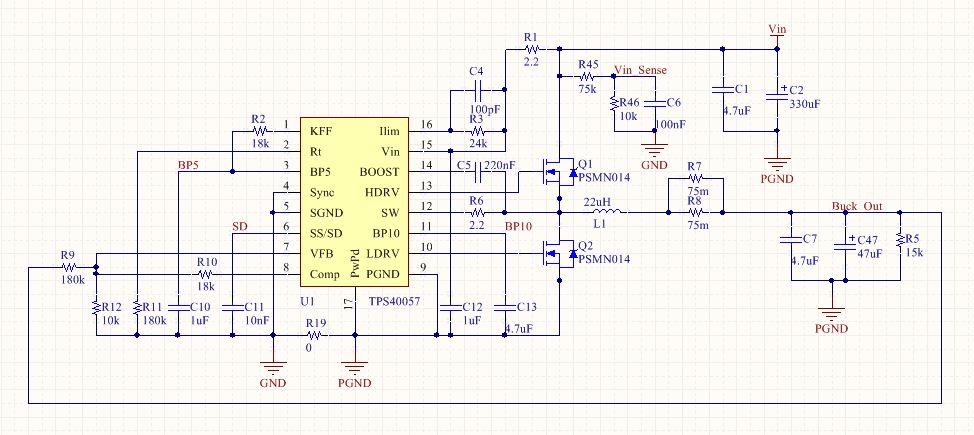
The schematic for the DC DC converter is the reference design shown in 40V_Power_Stage_Board_PMP5306_RevD5.pdf. I am using the DC DC as a battery charger. I am trouble-shooting the PWMIC to determine why there is no PWM pulse from the LDRV pin 10 or the HDRV pin 13.

I have some questions about what I should be seeing at the IC pins. 

The voltage at pin 2, RT,  is 2.4V DC -should this be a continuous DC or a ramp?

The voltage at pin1, KFF, is 3.49Vs, which according to the data sheet appears normal. This particular implementation does not use UVLO and simply connects the KFF pin to BP5, pin3, via a 17.5k ohm resistor. This gives an IFF of approximately 80uA. Since the resistor at RT, pin 2, is 180k, and the frequency of operation is approximately 300kHz, is this proper value IFF?

The voltage at pin 6, SS/SD, is approximately 3.5V -is this correct for operation? 

What can I do to determine what is preventing the PWMIC to pulse? I have checked all pins for noise or oscillation and have found none.

Will this chip run with the gate drive outputs tied to ground via a large resistor - say 10K? That way I could determine if the Mosfet gate inputs were the problem.

Thanks for your time.

  • Chuck,

    That you for your interest in TI parts.

    Can I ask you to post your schematic? The quoted ref design PMP5306 has a lot of other circuitry and I don't know how much of it you are using.

    Some answers:

    1) The voltage at the Rt pin should be a steady DC like you are measuring. The ramp is internal.

    2) This value of IFF is correct for the ref design but may not work for your application, depending on your input voltage. Please look at equation 2 on page 8 of the DS. What is your input voltage range?

    3) The voltage at the SS pin is correct and indicates that the device has already finished the soft start period.

    4) Yes you can add 10K to ground on the LDRV and 10K fro HDRV to switch node. But the FETs must also be present otherwise there will be no BOOST voltage for the HDRV.

    Please provide more details so we can investigate further.

    MC.

  • 7144.UBCpowerREV2.pdf

    Sorry for the repeat, I couldn't tell if the first upload went through.

  • I forgot to answer your question about the input voltage range. It is 22 to 32 volts.

  • Chuck,

    A quick calculation with that RKFF indicates that this is cutting it too close. It yields a min Vin of 4.988V if my calcs are correct. Try dropping the value of your R1 a bit, say by 15%.

    The whole purpose of this RKFF is to provide automatic line regulation, and it also combines in a UVLO function. I realize the ref design is connected as such (RKFF to BP5), but is there a need in your case to avoid using the normal RKFF connection?

    Are all the values in the schematic real? The values of RC1 and RC2 need revising.

    Also, there is a whole lot of other circuitry in the feedback network. I would suggest reducing the circuit to a simple regulator first, to make sure everything is working properly, then start adding the functionality back in block by block.

    MC.

  • Hi Chuck,

    Please share your findings on this issue. Also, do you know why is the current sensing resistor placed before the output capacitor? Is it intended to sense the inductor current and not the DC current?
  • Hello Paul,
    We fixed this issue by not using the UVLO feature of the TPS40057. We used a separate circuit for this function. That way the input voltage would not shut off the IC.

    As far as the sense resistor placement goes, I am not certain why the sense resistor is placed between the output inductor and the output capacitor. We did not try to moving it to the output. I would guess that there would be less ripple noise across the sense resistor, however you would have an extra pole in the feedback loop due to the output capacitor. We didn't have time to experiment with this question, but it would be interesting to see how much it changes the loop gain of the converter when it is in constant current mode.

    -Chuck
  • Hi Chuck,

    I'm currently having trouble to regulate to my desired output. Attached is the schematic of buck section. Once the IC start switching around 8V input, it only regulates at ~3V output. VFB voltage is 0.7V Switching frequency is correct around 300kHz. Did you encounter similar problems before?

  • Hi Paul,

    Our design is complete and we have delivered product.

    I don't think your problem is with the feed-forward network. I think your problem is with the error amp compensation network -R10, R9. You have the feedback resistor, R10 at 18K and the input resistor, R9, at 180K. The ratio of R10 and R9 is less than one, which makes the error amp a non-inverting gain block with a gain of 10, so that at 3.0V output the voltage at VFB is 0.7Vs. This is the only solution you can get if you have the error amp gain set at 0.1 inverting with a reference voltage at 0.7 V.

    Usually R10 has a capacitor across it to give the error amplifier maximum gain at DC. 

    You need to look at the data sheet and follow the Loop Compensation design guidelines, section 7.3.8 on page 13.

    Chuck 

  • Hi Chuck,

    Thanks for your quick reply. Yeah I realized that too. I just followed the slaa476 reference design and BoM that's why the value of R10. I just use R9 -180kohm to power-up the buck section. Now I will try to change the feedback network values.