This thread has been locked.

If you have a related question, please click the "Ask a related question" button in the top right corner. The newly created question will be automatically linked to this question.

BQ3055 battery management- Isolating GND

Other Parts Discussed in Thread: BQ3055

HI,

For the BQ3055 battery management design, we have connected the electrical gnd of the battery negative terminal to the battery management chip and its associated circuitry and a separate analog gnd for the point of contact to the charger kit.

Should the analog gnd for the point of contact to the charger kit  be same as the gnd  of battery management chip and its associated circuitry and a seperate gnd for the battery negative terminal or should it be the like the one i have stated in my previous comment
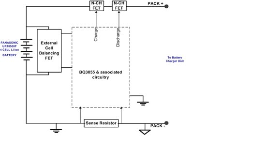
i have attached block diagram of both the representations and let me which one is correct

Block Diagram 1          

  • Vikram,

    The ground for the device (VSS) and associated external components should be connected at the negative terminal of the battery cell stack and shown in your first diagram. The connection should be made close to the cells to help to minimize a voltage drop due to current flow through the PCB and sense resistor. (quiet ground connection)

    Tom

  • Hi Thomas,

    Thanks for your response.

    Adding two more queries:

    1) For using external cell balancing circuit, is it recommonded to use P-CH FET part with body diode as the body diode might cause a reverse bias condition or FET part without body diode.

    2) what's the logic behind the use of "2N7002" in the circuit?

  • Vikram,

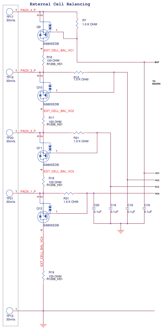
    Are you referring to the external cell balancing circuit example in the datasheet? If so, I reviewed the diagram and there appears to be an error. The external p-channel FETs should be oriented with the source towards the top, instead of the bottom. The diode represents the body diode and it is oriented properly. Also, the internal FETs should be n-channel. We will correct the drawing. If this is not the circuit that you were referring to, then please let me know where it is located.

    Regards

    Tom

  • Hi Thomas,

    1) Yes i was referring to the one on the datasheet.

    For the external cell balancing, the external P- Channel mosfet source is connected to the "VC" pins of the BQ3055., ie drain of the internal n- channel MOSFET.

    During cell balancing, the source voltage of the external p-channel will be zero as the mofet will be conducting through the current limiting resistor

    I have attached snap shot of the circuit. Could you please tell me if it is correct.

    2) As i have stated in my previous mail, could you tell me the logic behind the MOSFET connected to the DSG pin , ie 2N7002 part as in application schematics.

  • Vikram

    Your cell balancing schematic is drawn correctly. The 2N7002 FET is used for reverse protection in the event that PACK+ is pulled below PACK-. It will disable the DSG FET.

    Tom

  • Hi Thomas,

    Thanks for your feedback.

    Could you please share information regarding sample SMBus test code (in C format) that is available for validating the BQ3055 as the EVM comes with PC software.