


Hi,
Form previous help in this forum, I had successfully generated +100V output from +12V by using TPS40210 in a TINA simulation.
( TPS40210 cannot boost up to 100V output )
My next step is to generate both +100V and -100V from +12V input. As I know flyback topology is a common choice, I started from flyback but met some problems.
1. TINA simulation
Schematic as below(also attached the simulation file), it seems the circuits below works fine, but a 1:10 transformer can only boost +12V up to about +/-60V at VOUT+ and VOUT-.
If I change the transformer winding ratio to 1:20 I can get +/-100V output, but is it a correct result ?
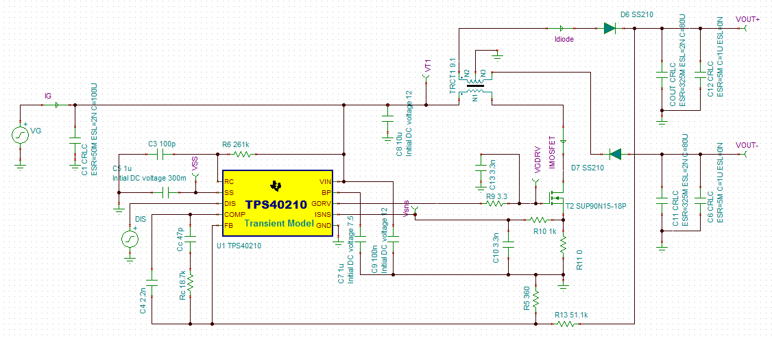

5621.TPS40210_100V_flyback.TSC
2. Real circuit test
I've got a sample transformer(winding ratio 1:9.1, 1212.CT8597-AL客户规格书.pdf ) and I did some jump wire on TPS40210 evaluation board to realize the above circuit.
My testing results shows that I can only get about +35V at VOUT+ and -20V at VOUT-, and in this case the input current at 12V is toggled between 0.3 and 0.8A, meaning that the power conversion efficiency is pretty bad(there is no resistance load at VOUT+ and VOUT-). I cannot get higher output voltages because the external MOSFET starts to be burned out if I try to adjust R5 for higher voltages. See below picture :
- Yellow : gate driving signal of TPS40210, showing that TPS40210 is continuing switching the external MOSFET
- Blue : 12V input current measured by a current probe(1V = 1A), showing that the input current at 12V is toggled betwen 0.3 and 0.8A

So, two main questions :
- Do I need a 1:10 or 1:20 winding ratio transformer to get 12V->+/-100V output ?
- Why the power conversion efficiency is so bad in real circuit test ? This is not the case when I did TINA simulation.


