This thread has been locked.

If you have a related question, please click the "Ask a related question" button in the top right corner. The newly created question will be automatically linked to this question.

TPS23756 Problems, EVM design files

Other Parts Discussed in Thread: TPS23756, TPS23754EVM-420, LM431, TL431, TLV431, TPS23754

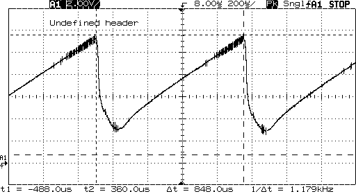
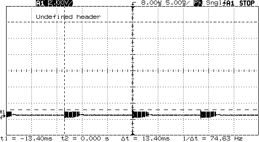
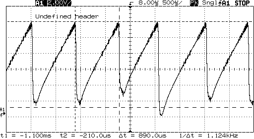
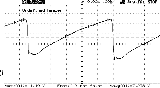
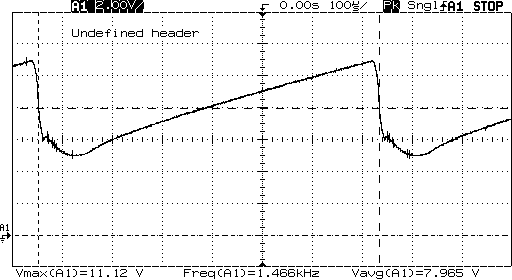
I'm currently trouble shooting a design based around the TPS23756.  It is based on a mix of the various flyback reference design for this series of parts, and is to have an output of 5V/3A.  The result I'm getting on the output is a sawtooth wave from 2V to 12V at a frequency of 1kHz (screen shot attached).  I've double checked the math for all components and made some other tweaks, however I'm having no luck.  If anyone has any suggestions as to where to begin looking it would be appreciated.

Are schematic and layout files available for the boards used in SLVA475 and SLUA469?  I realize these are very different designs, but if I can't resolve the issues with my board quickly I'm considering just rehashing my design mimicking SLVA475 as close as possible, while also introducing elements of SLUA469 to make sure the EMC is clean.

  • If you can post your schematic, I can see whether anything jumps out. From the looks of the waveform, feedback loop stability may be the issue. We can start with the schematic review, and then explore other designs if necessary.

    Are you using TPS23756 because you have a low voltage adapter input voltage requirement (and output power above POE class 3 limits)? Native schematics and gerber files are available for both SLVA475 (uses same layout files as contained in TPS23754EVM-420 EVM user guide online) and SLUA469. Let me know which you prefer.

  • Are you using TPS23756 because you...

    My interpretation of the difference between *754 and *756 was the UVLO on Vc, which is supplied by the bias winding of the flyback transformer.  As I calculated my bias voltages to be 12V or less I designed in the *756 since the *754 has a UVLO of 15V (rising), which is greater than my anticipated bias voltage.  I anticipate my adapter voltage to be as low as 20V.  My output power requirements for the current design are no more than 13W, however I do anticipate reusing whatever TPS2375x controller that makes it into this design in future designs, which may be up to 25W.

    Native schematics and gerber files are available... Let me know which you prefer.

    I'd prefer SLVA475.

    If you can post your schematic, I can see whether anything jumps out.

    I have three variants of the same base design using three different transformer cores.  The EP13 and EFD15 variants have similar outputs.  The EFD20 variant I fired up yesterday for the first time, isn't doing much of anything, and I admittedly haven't had much of a chance to trouble shoot it. 

    EFD15 Schematic

    6862.AAM_EFD15_SCHEMATIC.pdf

    EFD15 Waveform

    EFD20 Schematic

    1134.AAM_EFD20_SCHEMATIC.pdf

    EFD20 Waveform

    EP13 Schematic

    0131.AAM_EP13_SCHEMATIC.pdf

    EP13 Waveform

  • We have a pretty good POE flyback design application note to help guide you through component selection and also transformer design (http://www.ti.com/general/docs/lit/getliterature.tsp?literatureNumber=slva305c&fileType=pdf). I am also attaching the PCAD schematic and PCB/Gerber files for TPS23754EVM-420 and PMP6672B. PMP6672B starts with the TPS23754EVM-420 and makes 10-11 circuit modifications to arrive at PMP6672B. So, the layout is the same for both. In SLVA475, the component changes are tabulated (changes are also listed in the lower left hand corner of the schematic).

    Suggestions based on the schematics: 1. Remove the capacitor from the CTL pin to GND. This is probably the cause of the instability. 2). You may need a resistor between the CS pin and the current sense resistors for additional slope comp (when Vin is low and the duty cycle is high). See the explanation in the datasheet. 3) Start with and/or compare component values against the EVM (or PMP6672) for starters and then you can adjust from there. 4) I did not have a chance to compare the flyback transformer specs of your parts vs. the EVM specs. Compare pertinent specs to see if any large differences appear.

    You are correct about the difference between '756 and '754. Vc UVLO is higher for '754, but you can still use '754 with a 12V bias voltage. '754 can operate with 24V and higher adapters while '756 can operate from a 12V (and higher) adapter voltage. Each part bootstraps the VDD1 voltage up to UVLO rising during start up and then the converter starts and the bias winding takes over maintaining Vc above UVLO falling (~9V for '754).

    TPS23754EVM-420.zip
  • We have a pretty good POE flyback design application note...

    Yep, went through it before looking for help on here.  In the previously posted schematics the red lined discretes are the result of running through the calculations of the app note using Python.  One thing that is a bit fuzzy for me is:  what is an acceptable phase margin?  50 degrees plus or minus something?  Does one need to mind the magnitude of FB?  Is f0 always 5.5 kHz?

    Suggestions based on the schematics...

    I removed the cap from CTL to ground, and I'm still unstable.  I added a 3k resistor between CS and the CS resistors.  The waveform changed some, but I'm not entirely sure how to read the change (for better?  for worse? indifferent?).  I'll insert the screen shots at the bottom of this response.

    Start with and/or compare component values against the EVM

    I have samples of the transformer for the original TSP23754EVM-420.  Tomorrow I'll build up a board from scratch replicating the components as much as I can.


    Original circuit (500 us time division)


    Cap from CTL to ground removed (100us time division)


    Cap removed from CTL to ground and slope comp resistor added (100us time division)


  • A colleague of mine noticed a few items in your schematic:

    1. U2 is LM431 (2.5V reference) and with R28/R29 values your target output voltage is (33k+10k) / 10k x 2.5V = 10.75V. For 5V and 3.3V applications we normally use an error amp with a 1.24V reference to provide more regulation "headroom".

    2. C22, soft start cap can be a bit larger (0.47 to 1uF).

    3. For the feed back opto-isolator, we try to use a part with a more limited CTR range. The HCPL part will have a 1:3 range and a TCMT or FOD type part used on the EVMs is more like 1:2. This factors into loop gain.

    4. For protection between VDD and VSS we use a 58V TVS. In at least one schematic, that TVS is between VSS and the AUX input.

  • 1. That's a whoopsie on my part, not realizing the TLV431 and TL431 had different references.  I put in a sample request for TLV431.

    2. In my attempt to modify the assembly of my PCB to replicate the TPS23754EVM-420 I have upped the soft start cap to 1 uF

    3.  I'm not entirely clear on how to read the optocoupler datasheets and conclude your numbers.  I see that the HCPL part the CTR can get to about 120%, and the TCMT part can get to 100%, but I'm not seeing anything in the datasheet that sticks out to give the 1:3 and 1:2 ratios.  Is there anything in the TPS2375x datasheet that would have clued me in as to the appropriate CTR ratio?

    4.  the power supply schematic as I've posted it plugs into another board that has the diode bridges, Ethernet connector, AC/DC rectification, over voltage protection, and PTCs

    Thanks again for your continued help.  I build up a board from from the ground up to replicate the TPS23754EVM-420 as much as I could with parts on hand.  Unfortunately it won't start up.  Since my layout doesn't match the EVM there's quite a bit of jury rigging, so there is plenty of room for error.   I have the transistors and diodes used in the design on order.  I won't have a chance to continue trouble shooting until Friday.  As I've been at it for a month now with this design if I don't manage to reach a resolution come Friday I'll more than likely scrap the design and replicate the TSP23754EVM-420 layout.

  • An update:  I did what I could to replicate the TPS23754EVM-420, and I am unable to get the board functional.  Voltage is going to where it needs to be, and the controller is trying to drive the gates, but there is no output from the over all supply.  There is a bit of jury rigging to my board to get it to match the EVM, so the room for assembly error exists.  Even if I did get it working, the amount of jury rigging required (stacking components, removing solder mask to add new parts, etc) makes my existing boards impractical for making multiple prototypes for initial development.  Since I've been at this for a month I'm going to cut my losses and spin a new design that faithfully replicates the EVM.

    Thanks again for the help you have provided.

  • I'm sorry you couldn't get it up and working. It may very well have all been layout related. There are many good layout guidelines in the various EVM user guides and I would especially recommend the EMI layout guidelines contained within SLUA469 (accessible from the TPS23754 or any of our PD product pages).

  • Thanks for the tip.  My plan of attack is to replicate the TPS23754EVM-420 layout, and then review the EMI layout guidelines and make any modifications based on that document's recommendations.

  • A slight change in scope is forcing me to switch from 5VDC to 3.3VDC.  Are there known mods to the TSP23754EVM-420 to adjust it to 3.3VDC?   Or am I better off just implementing the 3.3VDC forward converter design (http://www.ti.com/tool/pmp7452)?

  • PMP7452 is a proven design and I would recommend this approach. FYI, PMP7452 uses the PCB layout from PMP5818 and is available from the TI web site. Let me know if you need gerber files or native (PADS) layout.

  • Native PADS layout for PMP5818 would be very helpful please.

  • Please find the PMP5818_RevB .PCB file attached.

    PMP5818_RevB.PCB
  • I just noticed that this format is actually PCAD 2004 instead of PADS. Will that format still work or should I send the gerber files too?

  • PCAD works just fine.  I'm designing in OrCAD, and have a viewer for PCAD.  Thanks!

  • Can someone verify if C101 is represented correctly on the schematics for PMP7452?  The schematics show this cap going from Pin 1 of the forward transformer to the secondary ground.  However, when looking at the photo of the board in the report for the design (SLVU848) it looks like C101 tied to the primary ground, not the secondary ground.  Which is right, or which way is it supposed to be?

  • C101 is represented correctly in PMP7452 schematic. C19 bridges secondary GND to primary RTN. Note that PMP7452 was built on a different PCB (PMP5818) and so the photograph may be a bit differeent.

  • You've added some extra confusion in there for me.  I'm not entirely sure what you mean by it "PMP7452 being built on a different PCB."  Different than what?  I thought both reference designs PMP5818 and PMP7452 were built on PCB PMP5818 revB?  The reports for each design (SLVU840 and SLVU848) have photographs of the built up boards with "PMP5818 REV B" clearly marked at the top of the boards.    

    Not to be stubborn or argumentative here, but when looking at the picture on page 4 of SLVU848, there is a capacitor kluged in from the top of C11 to the left of C19.  I assume this is C101.  Looking at the PCAD file provided in this thread (PMP5818_RevB.PCB), neither one of those nets is secondary ground, which would imply that C101 was cut in contrary to the schematic.

  • Sorry for the confusion, Randy. You are correct that PMP7452 and PMP5818 are both build using PMP5818 Rev B PCB as the photo's show. And, now I can see what you are referring to about C101. C19 can be seen in SLVU840 photo just below T3 to the left of "Q5" text. The right side of C19 connects to secondary GND and the left side of C19 connects to primary RTN or ground. In SLVU848, C101 is just to the left of C19 and appears to be connected from primary RTN or ground to T3-1 which is not in agreement with the schematic. Please follow the schematic connection for C101.

  • Thank you for confirming my observation and for advising that the schematic is to be followed over how the board was assembled.