This thread has been locked.

If you have a related question, please click the "Ask a related question" button in the top right corner. The newly created question will be automatically linked to this question.

Problem in tps54160

Other Parts Discussed in Thread: TPS54160

Hi,

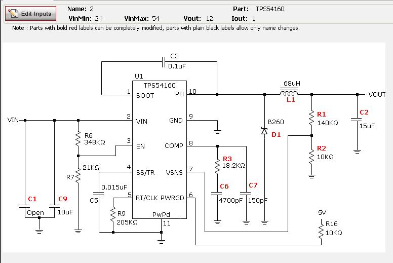
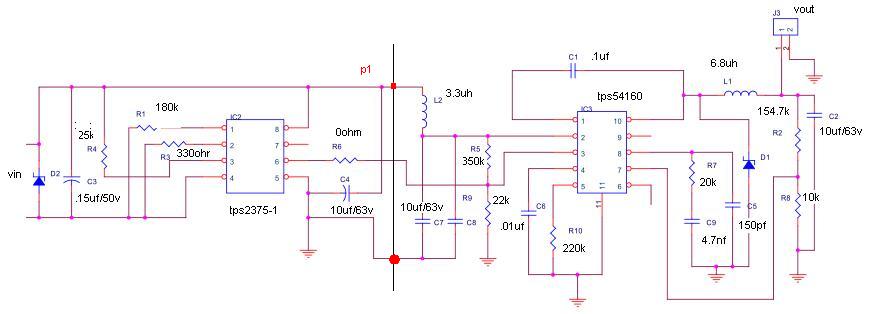
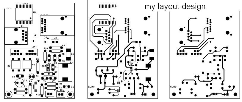
I  have designed one circuit for TPS54160 from the reference of www.ti.com/lit/ml/slur225/slur225.pdf and switcher pro recommended ( attachments). i attached my circuit with this post also. i get  50v output at p1. but no output at Vout. can any one suggest me the issue here.

  • Hi Fazlur,

    One thing I noticed is pin 9 is not connected to anything in the second schematic but this should be connected to ground. Is the schematic correct?

    Best Regards,
    Anthony

  • sorry i failed to mention that.

    I connected that 9th pin to ground.

  • Hi Fazlur,

    From looking at the schematic, there is nothing which looks to be an issue with the component selection for the TPS54160. I did notice SwitchePro suggested a 68uH inductor while it looks like you are using a 6.8uH inductor.

    To help understand the issue I would like to see some more description of what the TPS54160 tries to do with 50V on the input. For example do you see any switching at the PH pin? Also what does VOUT and VIN look like on an oscilloscope?

    *EDIT* What type of input capacitors are you using? At least 1 ceramic bypass capacitor is required and this should be placed as close as possible to the VIN pin with the shortest return to the GND pin as possible. It should be of type X5R or X7R dielectric. The 10uF/63V rating makes me think it is not ceramic.

    Best Regards,
    Anthony

  • Ya Anthony, you are correct. i thought that was just input filter capacitor which we use in normal voltage regulator like LM78** series.  OK  I'll try that with ceramic one.

    But i used 68uh inductor . wrongly i mentioned that...

  • Hi Anthony,

    Please make me clear about the capacitors. Because in my locality. some range of capacitors are not available. wrongly i used capacitor types. So please specify the capacitor with that type(electrolytic, tantalum, ceramic...)

    C6    0.015uf                      // i used 0.01uf ceramic

    C7    0.1uf/100v?              //  i used 10uf/63v electrolytic, you mentioned that as wrong. then what is correct for that

    C2     15uf                          //  I used 10uf/63v electrolytic

    C9     4700pf                     // I used ceramic  

    C5     150pf                       // I used ceramic

    C1      0.1uf                       // I used ceramic  

    C4     0.15uf                     // I used electrolytic 0.15uf/50v

    So if there any changes means please suggest me.

    Do you have a verified circuit for my issue?

  • Hi Fazlur,

    It is highly recommended to place a ceramic bypass capacitor very close to the VIN pin to provide good decoupling. A 0.1µF can be sufficient if there is some bulk capacitance in parallel.

    I did not see anything wrong with looking at the component values in the schematic. You may want to try reducing R7 (maybe 15k) and increasing C9 (maybe 6800pF) to lower the bandwidth of the control loop. Can you share some oscilloscope screenshots of the VIN pin, VOUT and the PH pin? I cannot say much without looking at screenshots.

    Lastly I am guessing this was created on a custom layout. Please see Figure 65 on the datasheet to compare the layout of your board to our recommendations. Layout is very important for switching power supplies.

    Best Regards,
    Anthony

  • Hi Anthony,

    you are correct. My layout is entirely different from that. I thought that wont create this much issue.

    So the final thing is, I should re-module my design. I have attached my design in this post.