This thread has been locked.

If you have a related question, please click the "Ask a related question" button in the top right corner. The newly created question will be automatically linked to this question.

UCC28600 Design Question

Other Parts Discussed in Thread: UCC28600

When I have done large scale modeling in the past for fix frequency PWM converters I have averaged them over 1 switching cycle to obtain a model that will provide losses of the various parts of the design.

It has been pretty handy for the DC modeling.


For the Variable Quasi-resonate supply, I’m not sure how to model the Large Signal DC, and or small signal model for this type of supply.

I believe the UCC28600 Mosfet Conduction time is Variable, as the load increases the frequency reduces.

The min would be typically 40 KHz possible from the UCC28600.

I’m want to solve for the Primary inductance needed for my application, and understand what the Operating frequency will be between the Min and Max voltage ranges.

I was thinking 100V to 400V.


I think the design approach would be to assume 40 KHz, at Vmin at full load power with me deciding on the Ton /Toff ratio.


Once I have that I can solve for the Inductance.

But if I wanted to model the performance of the supply and its expected frequency due to supply voltage, and load, how do I do that?

  • My advise is to use the Excel Design Calculator that can be found in the UCC28600 product folder in the software section (slvc104). 

    This design calculator takes the users inputs and performs macros that take into account the transitions from frequency modulated mode where the peak current is fixed and the frequency modulates depending upon line and load conditions, amplitude modulation mode where the frequency is fixed but the primary peak current is modulated depending upon operating conditions, and finally the line and load conditions where both the frequency and the primary current is modulated for transition mode operation.  The displays on the QR Simulator page graphically display the switching frequency, feedback voltage, and primary peak current as line and load changes.

    Also note that it is not recommended to design the primary inductance to switch at 40kHz at minimum input maximum load as there will be timing issues with the internal QR Done signal and extraneous gate pulses will result.  The design calculator limits the minimum switching frequency at min line max load to 80kHz.

    You may also refer to Green-Mode Power by the Milli-Watt, which was a topic for one of our power supply design seminars that discusses designing a QR flyback converter (http://focus.ti.com/download/trng/docs/seminar/Topic2MM.pdf)

  • Don't know whether this is the right place, but I am struggling with erroneous gate pulses coming out of the UCC28600 and the remark above made me curious. 

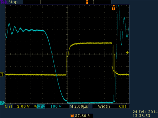
    In my design the UCC28600 creates a short pulse (spike) after the gate went low whenever the on time is greater than 7.4us. The whole switching period is 18.8us, so still far away from 40kHz. The length of the erroneous pulse is about 160ns and comes exactly 220ns after the gate signal has gone low. I did not find a way to remove it. All other signals are in their range (2V < Ufb < 3V). If the vertical repeat time of your scope is too slow you won't see the pulse and think it's just one edge.

    Any additional information concerning the above mentioned 'extraneous gate pulses'? Under what conditions do they come out of the chip?

  • The erroneous gate pulse isn't limited to 40kHz but is a function of the on-time.  As a rule of thumb, keeping the switching frequency greater than 80kHz when the operating conditions are minimum input, maximum load will usually result in an on-time that is less than 6.5us.  So the fact that you are switching at 53kHz, and not 40kHz, under these conditions is not enough to avoid this extra gate pulse.The fact that your on-time is 7.4us means that your converter is on long after the internal signal that tells the gate NOT to turn on if it "sees" a valley has expired, so any perceived change in slope on OVP will tell the controller to initiate a gate pulse, even if that "valley" is the result of the slug of energy from the Gate drive itself turning off.  Designing the transformer so that the on-time at minimum input, maximum load is less than 6.5us.  The easiest way to do this would be to use the recommended inductance calculated with the design calculator that limits the switching frequency to 80kHz at minimum line, maximum load.

  • Thanks for your explanation. I read your recommendation of putting the frequency up to 80kHz but the chip shall be a replacement for an existing so I am a little bound to some limits.

    In addition I want to understand the behavior so I took a closer look to the chip: First I think the output register CLK must be connected to the Q and not the /Q for correct operation. If I use that CLK I understand the following: In QR mode ( 2V < Ufb <5V) ON/OFF is just determined by current limit and QR-DONE. The oscillator swings between anything above 1.4V and 0.1V, so it is hot for QR_DONE detection earliest after 7.7us.

    The screen shot below shows that the small drain raise probably triggers the gate pulse which would be exactly what you mentioned. But then I do not understand the drawing for the QR_DONE detection: as long as Udet is below ground the AND gate cannot become high? (BTW the OUT should be a /OUT).

    Nevertheless, under your described conditions the chip is not working for us.

    Thanks for pointing out the reason, I was really frustrated that I did not find the reason though I searched hard for some time. Please put this behaviour into an errata sheet to avoid such situations. This was the first what I was looking for. It could have saved me a lot of time.

  • ...sorry, mixed this up, you're right: The AND is active when Udet if below 0.1V so the small raise of the drain voltage  leads to a gate signal :-( Thanks again!

  • To my opinion it is important to tell your customers that under no circumstances pulses longe than 7us are allowed for operation. Otherwise under worst case conditions the erronous gate pulses put additional stress to the MOSFET. This is NOT clear when reading the data sheet (first writer also wanted to use 40KHz as lowest frequency).