A related question is a question created from another question. When the related question is created, it will be automatically linked to the original question.
If you have a related question, please click the "Ask a related question" button in the top right corner. The newly created question will be automatically linked to this question.
Thank you for sending all the pertinent information in the message. If you are seeing failures on power up, then you might have a very noisy input which is damaging the IC. I have listed the following issues that should be corrected on your board:
1) From your schematic it looks as if there are only two filter caps viz. C16 and C14 at the input. You should have some bulk capacitance also in addition to the filter caps. Additionally, the filter caps at the input should be placed very close to the Vin pins and PGND. This helps bypass the noise and reduce spiking. If they are placed further apart then they are not doing any good. Webench might not show the bulk capacitance in the schematic and show only the filter caps.
2) The FB divider is not close to the FB pin. The FB node is a high impedance node and making long runs to it is not good because more noise can be coupled on to it. Having the FB components closer to the pin would help.
3) You should remove all relief connects on your board. Relief connects add more inductance. Having continuous copper pour is desirable.
I would advise you to follow the layout tips from the datasheet. I hope this information is helpful.
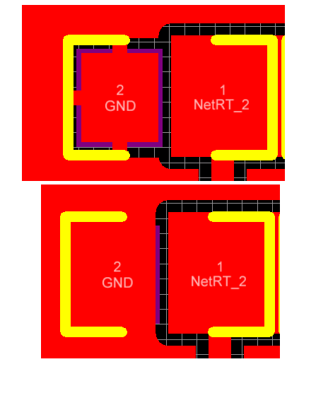
Thank you for more information. The "relief connect" and "direct connect" terms pertain to the way the copper is poured on the board. Relief connect isolates the component pad from the copper pour area so as to make it easy to solder the component. The pad is connected to the copper on the board through a narrower trace. The thin traces in turn add more inductance in the path and cause spiking. Direct connect does not isolate the component pads and therefore does not add more parasitic inductance. I have attached an image showing the difference. In the attached file, the upper image is an example of using relief connect and the lower image is an example of using direct connect . You should use direct connect.
Another thing I had mentioned in the previous message was that the Vin bypass caps (in your case the 1uF and the 100nF caps) should be directly across Vin pin and PGND. The PGND should be connected to the DAP directly. In your layout, the Vin bypass ground is going through a via. Adding a via again adds more noise in the HF current path. Ideally all the switching currents should be contained in the top layer. On your layout the HF current is travelling a very long path. I have attached a presentation explaining the good practices for board layout and mitigating EMI ( 0878.Switching Power Supply Design_ EMI.ppt ). The AGND and PGND pins should be connected to the DAP under the IC as well. It does not seem so from your layout. You would still need some bulk capacitance which can be a little away from the Vin pin, but not too far. Here is a link to a similar post that was answered in the past (http://e2e.ti.com/support/power_management/simple_switcher/w/simple_switcher_wiki/2261.problem-with-lm5576-pcb-layout-issue-dies-on-short-circuit.aspx).
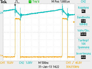
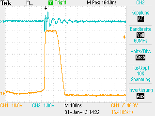
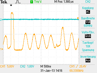
The Ccomp and Ccomp2 caps should not be swapped. But if they are swapped, you will have an unstable output or the design will not regulate at all. But the chances of it destroying the IC are very low. The last waveform you added shows the DCM mode. At very low loads or no loads, the converter enters the discontinuous conduction mode. The switch will not be a perfect square wave in DCM. I hope this helps.
In my previous email I sent you a presentation on EMI and ways to mitigate EMI using good practices in board layout. In that presentation, on slide #58, there is an excel spreadsheet embedded which will help you calculate your filter components. I would suggest using one 10uF ceramic cap as an input cap and one 1uF ceramic cap as bypass cap which goes right across VIN and PGND. Using these values you can then calculate the values of the filter components including the bulk cap.
The DAP stands for die attach pad. It is the metal slug at the bottom of the IC. It needs to be connected to the PGND and AGND pins and should be flushed with copper as it is also used for heat sinking. The LM5576 is a robust simple switcher part with a max input voltage of 75V and max output current capability of 3A. Therefore I do believe that the LM5576 is a good choice for your requirements.
The layout for the LM5576 eval board could be better. But the way it is done is also not too bad. The Cin ground and the diode anode are connected on separate layers, through a lot of vias. Having more than one via and arranging them in a form of a matrix is also helpful. In a situation like this the board should be made with 4 layers. The second layer should be all ground without any traces. Therefore if the high frequency current has to routed through different layers, it flows un-impeded on the second layer.
I am sorry, but I cannot answer the questions regarding the LM3404. The LM3404 is a LED driver and you should re post your question to the appropriate forum (http://e2e.ti.com/support/power_management/led_driverslcd_bias/default.aspx).
Just for your information, the LM3404 is featured on Webench LED designer. You could create your design using the LM3404 on Webench very easily.


