This thread has been locked.

If you have a related question, please click the "Ask a related question" button in the top right corner. The newly created question will be automatically linked to this question.

Regarding boost converter with TPS40210

Other Parts Discussed in Thread: TPS40210

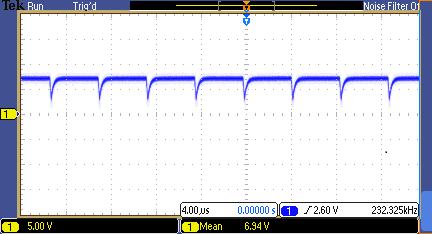
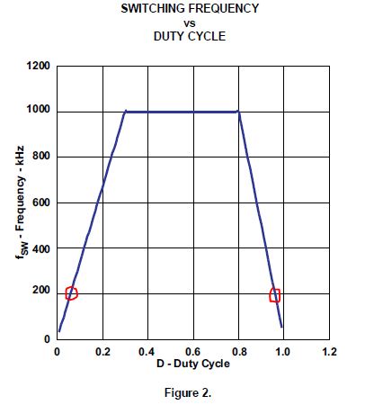
I have designed boost converter with TPS40210.

Vin(min)=20V, Vin(max)=40V , Vout=200V Iout=2A

But my design is not working. As per the datasheet this IC support up to 260V Vout.

For designing I used IC datasheet design steps and found out the component.

Can anyone please tell me what are the main components I have to check again?

Appreciate your help & support.

Amruta

  • Hi Amruta,

    Can you please share your schematic and waveforms of what the TPS40210 tries to do? I am curious of input voltage, output voltage, ISNS voltage, the gate drive voltage of the FET, and the drain to source voltage of the FET.

    Are there any input voltage and output current combinations in which the output voltage does regulate? This is quite a lot of output power requiring 20A of average input current if it were to operate with 100% efficiency. This requires a rather large FET.

    Best Regards,
    Anthony

  • Hi,

      Here I have attached my circuit diagram,8637.Circuit Diagram.docx]

    Circuit is not working so I could not get any voltage at ISNS pin or gate drive.

    IRFS4229PbF MOSFET is used  for the boost converter.If  I increase input from 20v to 40v I get same voltage at the output i.e. 20 to 40V.

    Yes there is requirement input voltage should be 20-40 and output current around 2A and output voltage of the converter should be 200V

    I connected this converter to H-bridge so at the output of H-bridge I need to get 115V/100W.

    Regards

    Amruta

  • Hi Amruta,

    Even if no load is present on the output, does the TPS40210 not turn on and regulate? I'm also not sure I understand the requirement of 115V/100W at the output of the H-bridge.

    It is possible you are pushing past the limits of the TPS40210 with this design. I do not know of any similar designs to yours using the TPS40210. However looking at your schematic there are a few things you will want to adjust in order to have a chance at this design working.

    First I recommend reducing your switching frequency. With what you have selected you are operating at 600kHz. In a high duty cycle applications a lower switching frequency has a better chance at success. Not including efficiency the estimated maximum duty cycle is (VOUT-VIN)/VOUT = 90%. The efficiency in reality increases the duty cycle. Please see Figure 2 on the datasheet.

    The lower switching frequency will also reduce the gate drive current necessary to drive your FET. With 72nC typical total gate charge, the estimated gate drive current needed is Qg*Vdrive*fsw = 72nC*8V*600kHz = 346mA. This is just below the typical value on the datasheet.

    Lastly the sense resistor might be too large for 2A output current, if you estimate 95% efficiency (this is just a guess with no calculations), the average input current will be 21A. Not including inductor current ripple the voltage across sense resistor will be 21A*10mΩ = 210mV. This is well above the 150mV typical over current value.

    Please see the applications section beginning on page 26 of the datasheet to help with your component selection.

    Best Regards,
    Anthony

  • Hi,

    1) I reduce frequency by changing RC pin resistor and capacitor. I got around 250KHz frequency.

    Still I don't get same problem. My output voltage is same as input.

    There is no voltage regulation I observed in it.

    2) Here I have attached gate drive pulses of MOSFET.It's duty ratio is not 50%.


    3) I refer the figure 2  in which for 200Khz , 0.1 or 0.9 duty ratio can be obtained,

    What are other parameters through which I can change the duty ratio?

    4) I used 1.2uF/450V output capacitor. I refer the design steps in the datasheet and got the value.

    but I think that value is too small to reduce the ripples. Is it affecting the output?

    Thanks and Appreciate your help and support.

  • Hi Amruta,

    Based on the waveform of your gate drive pulses you are at the maximum duty cycle limitation of the TPS40210. First you may try reducing the the switching frequency even further to see if it helps. You may also try replacing the series 3.3Ω resistor with a 0Ω to speed up the turn on and turn off of the MOSFET. The steady state SPICE models located in the TPS40210 product page could be used to test this out before testing on a real circuit.

    Also you might be misinterpreting Figure 2. The curves show the maximum or minimum duty ratio possible based on the switching frequency. With 200kHz switching the minimum duty ratio is about 0.08 or the maximum duty ratio is about 0.95.

    Lastly I do not think the 1.2µF/450V output capacitor is causing the issue of keeping the output in regulation. However it would definitely help to increase it to reduce output voltage ripple and voltage overshoot or undershoot in load transients.

    Hope this helps.

    Best Regards,
    Anthony