This thread has been locked.

If you have a related question, please click the "Ask a related question" button in the top right corner. The newly created question will be automatically linked to this question.

TPS5450DDA exhibits poor step load transient response

Other Parts Discussed in Thread: TPS5450

I designed a switching regulator circut using the TPS5450 regulator with a 24V nominal input and a 3.3V output.  I needed to support 5A for short term start-up (less tha 500ms) with an average current around 3A.  Initially, I designed the circuit using the classic energy balance equations with some inductor and output volatge ripple targets.  Later, I used the SWIFT software and found that the 10uH inductor I initially chose was increased to 22uH.  I selected a 22uH inductor with an Isat of 6.8A at a 10% drop in L.  I also used two 330uF, 25 mohm ESR capacitors even though the design only required one capacitor.  My hope was that since output ripple is the product of the inductor ripple current and the ESR I could reduce ripple and mainatin loop stability with the reduced ESR.

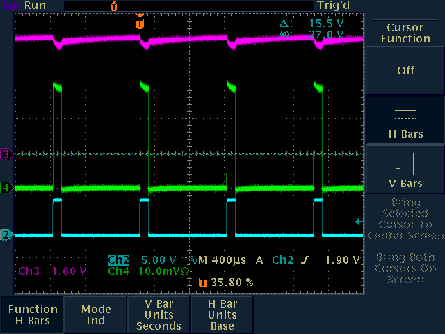
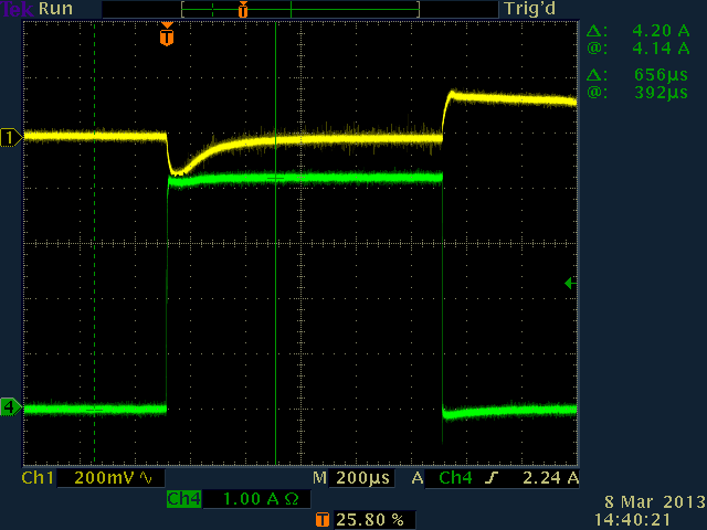
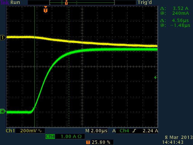
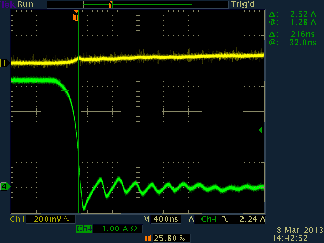
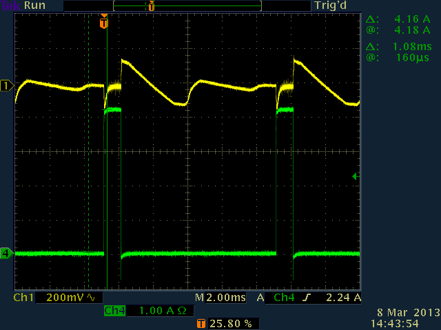
The problem is that when I subjected the regulator to a pulsed (10% DC at 1KHz) 3A load, I saw more than 160mV of load volatge deviation.  I measured using an SMA connector directly across the output capacitor and a direct coaxial cable connection to my scope so I believe I saw minimal B-field effects.  This much more deviation that I expected and I had hoped to have good load transient response up to 5A not just 3A.

I have a couple of concerns about my design but lack the experinece to know if these issues are the casue of my problem.  One concenr is that my layout loop that includes the TPS5450 PH pin to clamp diode and back to ground may not be small enough and could have some additional series inductance.  I modeled my design from the data sheet but later realized the reccomended layout in the SWIFT software was different.  Although I tried to use wide top copper areas for this node and loop, could too much series inductance in the diode path cause the poor load response?

Secondly, this regulator circuit is fed via an input filter network located on another assembly.  The filter includes a 10uH series inductor.  Of cource, I have low ESR ceramic input capaqcitors at the TPS5450 input but I see some ringing synchronous wit the load switching.  I used a scope probe with a low-L ground clip but my probing could be suspect.    At the switching regulator input pin, I have two 4.7uF, 50V, 0805 X5R capacitors.  I relaize that the effectve capacitance at the 24VDC bias is much lower than 10uF.   Could either my input capacitor selection, whih uses small package capacitors that exhibit degraded capacitance wit yh DC bias or my use of tghe remote input filter be the cause or a contributing factor to the observed poor load transient response?


Thank you in advance for any help or guidance. 


Craig

  • Transient response voltage deviation is usually determined by the output capacitance and ESR.  It will also vary with slew rate.  Fast slew rates can require quite a bit of low ESR output capacitance.  Can you post the waveform of Vout and Iout?

  • Hi John:


    I am new to the forum so hopefully I get this scope photo posted correctly.  The outpot vlatge is shown in purple at 1V/div, the load current in green at 1A/div and the blue is the MOSFET pulsed load drive signal.


    Thank you very much for your ehlp,


    Craig


  • That is good for a start.  I would like to see a zoomed in version similar to this:

    Where the top trace is the output voltage ac coupled and teh bottom trace is the current waveform.  I want to see the leading edge slew rate and the recovery characteristic.  If you are loading it with a FET switched load driven from a square wave, the rise time may be very fast.  I usually recommend 500mA / usec for "normal" amounts of capacitance.  Faster slew rates require more and lower ESR.  The disadvantage of TPS5450 is that it is intenally compensated.  The LC filter double pole and ESR zero frequencies need to align will with the internal zeros and poles for proper stability. 

  • Hi John:

    Unfortuantely, I do not have the assembly right now to give you the view you desire.  I will need to get this data later.


    When you refered to the LC filter double pole you were referring to the regulators's output L-C and not the input L-C I mentioned was located on the power input side - correct?


    Yes, I expect the di/dt of my pulse load to be very high - maybe on the order of 60A/us.


    Are you suggesting that I need to increase the number of low-ESR capacitors, using smaller capacitance values to acheive a very low ESR target?  What target value am I shooting for?  Is it true that the output capacitors essentially provide all of the initial load transeint energy before the loop itself has time to respons adjust the PWM?


    Thanks,

    Craig

  • That is a very fast transient, 100x faster than what I usually test.  You can estimate the the charge that is removed form the output during that time and how much capacitance is required to keep the voltage within your limits.  You may find it is quite a lot.  It may be that it will be difficult to stabilize TPS5450 for that large of an output capacitance.  It may be possible, especially if you can add a feed forward capacitor in parallel with the upper resistor in the divider network.  I can tell you that you would be better served with an externally compensated converter.

  • Hi John:

    I appologize for the long delay but I had to complete some other work.  Back to the issues with my implemenation of the TPS5450.  I was not vey clear in my past posts.  The test fixture I made had very fast rise and fall times; much faster than I required and I was naive about the implications to the design of the reguator especially since it is internally compensated.  The module is not yet available but I now have some current waveforms from the mfg that indicates it is about 2.5A in 50us or 50mA/us. 

    In any case, I modified my test fixture to at least slow down the leading edge of the MOSFET switch and have attached new waveforms in a form more like you requested. 


    I am now testing with a 1ms, 4A pulse that has a rep rate of 10ms.  The rising edge is now much slower at about 1.5A/us.  Not so bad on the leqading edge but problems on the falling edge (vertical at 200mV/div AC)


    but the falling edge is still very fast at about 20A/us


    If I look over a longer time, I see lots of loop instability as it seems to take about 8ms before the output starts to become stable. 


    Given that my target application may require slower a di/dt but needs to be able to handle at least 5A for short durations, do you believe I am ok with TPS5450?   Do you believe the poor transient response on the falling edge is beacuse of the high di/dt or poor matching of the output LC?   Earlier you mentioned lead compensation using a small capacitor across the upper divider resistor.  Will that improve my performance based upon what you see now?    If not, how do I best "tune" my output LC to match the internal compensation?  The data sheet shows that for the voltage mode type 3 compensation networ there are two zeroes at 2170 and 2590 Hz. and a first pole at 2165 Hz with many other poles much higher in frequency.  How do I takle the alignment?  Do I assume the 2165 Hz is the dominant pole and take the average of the two zeroes around 2400Hz.  I asume the output network looks like a series L feeding a shunt comboination of the output C in series with the capacitor ESR.    I can solve for the double pole and single zero but not sure what my goal is?


    Thanks for your help,


    Craig

  • Hi Craig,

    How much overshoot and undershoot are you hoping for? Will the transient in the real application be from full load to no load?

    A fast transient response from a full load to no load can present some large overshoots for non synchronous designs. The main reason is when the load is removed, the low-side switch cannot sink current to help return the output to regulation after the overshoot. Instead the device stops switching and the output voltage must decay through any parasitic load. The device will only start switching once the output voltage has began to drop below the target value and the voltage may drop too far before the loop can respond.

    I expect a slower transient will show significantly better performance because the loop will have more time to respond.

    Best Regards,
    Anthony