This thread has been locked.

If you have a related question, please click the "Ask a related question" button in the top right corner. The newly created question will be automatically linked to this question.

TPS40200 Must keep output switching off using SS Pin until 30 VDC input is available

Other Parts Discussed in Thread: TPS40200

Hello,

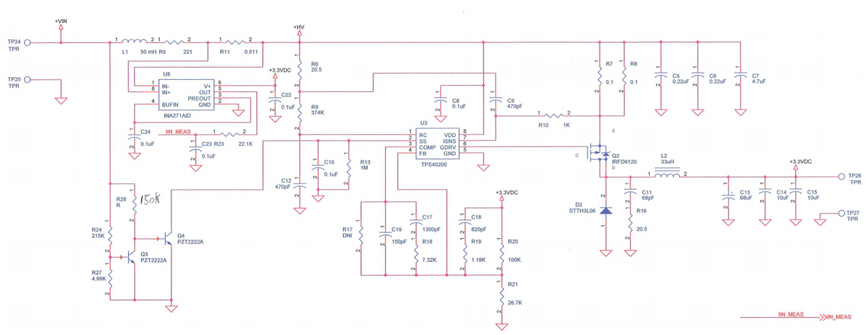
We are using the TPS40200 Voltage Mode Controller in a 50 VDC input voltage application.

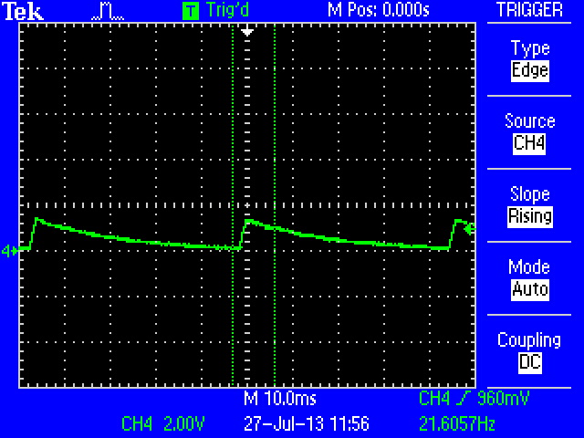
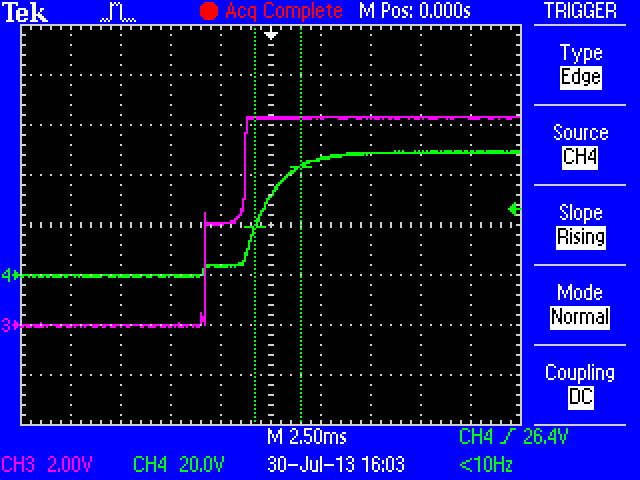
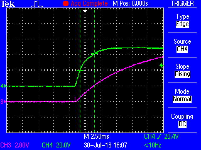
We must ensure that the output does not start switching (SS must be held low) until the input reaches 30 VDC. If SS is not driven low the output starts switching at an input of  ~5.5VDC.

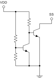
The voltages available for this hold down circuit are the 0-50 VDC. One idea was a comparator with one input fed by the input voltage through a resistor and held at a level using a zener diode and one input on a voltage divider fed by the input voltage. The VCC for the comparator would also be held through a resistor with the otther end tied to the input voltage using a zener. The initial problem with this is the VCC must reach at least 3 VDC before the the input reaches ~5.5 VDC so the resistor must be a fairly low value. The application is very low current and consumes too much current through the resistor and the zener. 

David Robinson


  • Hi Dave,

    One idea I have is the circuit below. When VDD is too low, the transistor on the right conducts pulling SS to ground. Once VDD pass the threshold determined by the resistor divider, the transistor on the left conducts turning off the right transistor and floating the SS pin.

    Any thoughts?

    Best Regards,
    Anthony

  • Hello Anthony,

    We prototyped it and adjusted the resistor values. So far so good. Thank you for the input.

    David Robinson


  • We have an application where we are using a transistor to as a switch connecting  30-50 VDC voltage to ground through what is currently a resistor.

    This network is used as a power line communications method. The voltage is not constant so we would like the current through the resistor to be a constant 500 uA.

    We need a constant current circuit in place of the resistor. Any suggestions.

    This is a high temperature downhole application.

    David Robinson   

  • Hi David,

    I personally don't know of a solution off the top of my head. Someone in the High Reliability forum might have some ideas though. They support the -HT versions of our parts so they are familiar with the down hole applications.

    Best Regards,
    Anthony

  • Hello Anthony,


    Previously we discussed a circuit that will control the TPS40200 through an SS pin connection.

    This circuit will turn have an output that goes high when the input voltage to the TPS40200 reaches approximately 30 VDC.

    The high transition on the SS pin will cause the output of the TPS40200 to begin the switching necessary to create +3.3VDC.

    I implemented this circuit and I am having a problem that crops up when the input voltage is intermittently interrupted.

    For example if the input is 50 VDC (then SS pin will be high) and I break and make the connection to this 50 VDC I can pretty easily get into a situation where the output is at ~1.5 VDC and I believe this is because the signal at the SS pin is not high and is oscillating. Please see the scope shot of this.


    I have tried disconnecting the transistor circuit to see if its output oscillates when disconnected from the SS pin and found that it does not oscillate.

    On the same token I have checked the SS pin for the oscillation once disconnected and found it ok as well.

    In fact the TPS40200 does not have a problem with the break and make situation if the transistor circuit is disconnected.

    Any ideas?

    David Robinson


  • Hi David,

    I'm surprised the transistor circuit is causing issues here. It appears the circuit is some how causing the part to falsely trip over current protection and get stuck in hiccup mode during the input transient.

    Can you share a schematic? Also a screenshot of the VDD voltage and SS voltage during the break and make situation may help. Both with and without the transistor circuit if you can.

    Anthony

  • Hello Anthony,

    I will start with the schematic.

    How do I send it to you, email?

    I am not sure I should post it publicly.

    David Robinson


  • Hello Anthony,

    Make Situation:

    This first image is the VDD (green) and SS voltage (violet) without the transistor circuit connected to the SS pin. 


    This second image is the VDD (green) and SS voltage (violet) with the transistor circuit connected to the SS pin.

    The TPS40200 entered hiccup mode after this image was collected.


    David Robinson


  • Interesting, so the hiccup mode is not entered right away. Does anything abnormal happen to VDD or any other signal when the SS voltage begins the hiccup waveform? It also looks like the transistor circuit is not holding the SS pin below 100mV until VDD reaches the threshold like it should.

    In the first waveform without the transistor circuit, is the 0.1µF cap still on the SS pin? The SS ramps up very quickly. The VDD waveform is also not very smooth in this screenshot, does it always look like this or is it a result of how the VDD power supply is turned on?

  • Hello Anthony,

    I agree it looks like the transistor circuit is not holding the SS pin below 100 mV until VDD reaches the threshold like it should. Perhaps this is because the transistor circuit is power up by +VIN in the schematic? +VIN is essentially the same thing as VDD though an inductor.

    The transistor circuit switches high when VDD is at about 26 VDC. I just found that if I slowly vary the VDD voltage around 26 VDC in the range of about 24 VDC - 28 VDC that I can pretty easily enter and get stuck in the hiccup mode. I found the only way out of this is to decrease the voltage and transition high somewhat quickly.

    In the first waveform mentioned above without the transistor circuit the 0.1 uF capacitor is not connected to the SS pin.

    David Robinson


  • Hello Anthony,


    This remains as a problem.

    Any feedback would be appreciated.


    David Robinson

  • Hi David,

    After taking a bit of a closer look at your schematic I noticed the filtering at the ISNS pin is a bit unusual although I can't think any major cause for an issue yet. The 20.5 ohm resistor is in series with the RC pin and with the filter cap to ISNS. The 470pF cap should be connected directly from ISNS to VDD. What happens if this resistor is 0 ohms instead?

    I also wonder if it was not disconnecting the transistor circuit which solved the issue but that you disconnected the 0.1µF SS cap. If there is only this 0.1µF with Q4 disconnected from the SS pin, does the issue appear again?

    Is there any load on the output? The 50mΩ sets the hiccup threshold at about 2A peak current. Which might be about 1.5A average load current not including any current needed to charge up the output capacitors during startup.

    Best Regards,
    Anthony 

  • Hello Anthony,

    We replaced the 20.5 ohm resistor with a zero ohm resistor and the result is the same.

    When Q4 is disconnected the situation is changed because the Q4 is the circuit that holds the SS pin low until the input is at 30 VDC.

    We did do another experiment with the SS pin after it was disconnected from the Q4. This was we connected the SS pin to ground after the input was at 30 VDC and then released it and we noted that we were able to get into the hiccup mode pretty easily in this setting. If we touched the SS pin to ground and quickly released it we went into hiccup mode.


    The load for this circuit is a microcontroller and some supporting circuitry that draws about 5 mA.

    David Robinson


  • Can you share the layout around the TPS40200? I can check if anything there provides a hint.

    C9 and C8 should be located very close to the IC for good bypass. On our EVMs the 470pF capacitor (C9) is right next to the IC's pins to improve the effectiveness.

  • Hello Anthony,


    Please see attached.

    C8 and C9 are close to the part.

    C9 is on the opposite side of the board.

    I have an TPS40200-EVM-002 board that this design was based upon and it does not have this problem.

    Richard Elmquist, Texas instruments helped me with the compensation network using the following:

    TPS40k Type III Loop Stability Design Calculator (Rev. C)  

     The layout was performed with the intention that is match the EVM board as much as possible.


    Please advise.

    David Robinson


  • Thanks for the layout David. Can you also add the copper and vias to the layout pdf?

    Looking at this there are a few things which could be causes. The FET is right next to the noise sensitive VDD and ISNS pins, even closer than the bypass capacitors. There is a good chance these are picking up the switching noise. If you look at the EVMs, C9 would be located right next to the two pins. Also C8 is right next to the IC similar to where R10 is currently placed.

    I also noticed the Inductor and FET are on opposite sides of the IC. How is the switching node routed?

    Are the snubber values listed on the schematic the ones actually used? Another thing to try without needing to change the layout is to increase the 68pF to 680pF to reduce the noise.

    One theory I have why removing the transistor circuit is causing nuisance tripping of the OCP is that it delays turn on to a higher VIN. At higher VINs there is more noise due to switching because the switching node is transitioning between higher voltages. The extra noise combined with the current needed charge the output capacitors is leading to OCP tripping.

  • Hello Anthony,


    The copper is attached.


    I am pretty sure the Inductor L2 and FET Q2 are on the same side of the IC but there is a mounting hole in between them. 


    The 68pF is the snubber value. I will try the recommended 680pF next.I agree with your theory. I will try testing it at different input voltage to see at what point the nuisance tripping stops occurring.

    David Robinson


  • I see now. I had overlooked L2 because of the footprint and was looking at L1. Some more comments below.

    • The VDD trace goes right underneath the FET, this is very likely getting extra noise. If you change the layout I would move the FET away from the TPS40200 and put the ceramic VDD cap right next to the IC with a short return path to the GND pin.
    • The switching node trace to the inductor is very thin. We typically make this wider to reduce the inductance.
    • The trace from the sense resistors R8 and R9 to the source of the FET is also very thin.
    • Please the ISNS to VDD cap right next to the two pins.
    • The SS cap and RC cap should return to the GND pin of the TPS40200 before connecting to the internal GND plane. This can be done by adding a seperate GND copper pour. This could also be used for the GND of the ceramic VDD cap.
  • Hello Anthony,


    We replaced the 68 pF (C11 which is connected to the drain of the FET Q2) capacitor with a 680 pF capacitor and noted no noticeable change in behavior. Please confirm we did this correctly and advise if you can think of something else to do in the realm of component value changes.

    I will try to see what VDD voltage value does not cause this issue on the existing board next. Perhaps we can set the transistor circuit to switch on at a lower VDD value to avoid this problem.

    Thank you for the input on the layout I will confirm it and as it turns out we may be turning this board in the near future.

    If we do perhaps you could look at this before we release the fabrication.

    David Robinson 

  • Hello Anthony,


    When VDD is reduced from 30 VDC which was desired to 17 VDC the hiccup mode probability drops considerably.

    You previously mentioned sense resistors R8 and R9. Did you mean the two 0.1 ohms resistors R7 and R8 instead?

    David Robinson

  • Hi Dave,

    You're right I meant the two 0.1 ohm resistors. I would be glad to take a look over the layout if you end up spinning the board. It's also good to see lowering the threshold improved the performance.

    Best Regards,
    Anthony 

  • Hello Anthony,


    I roached on multiple modifications.

    The problem was resolved when a wire was added shortening the node from the sense resistors to the Source connection on the FET.

    When we spin the board I will send it over for input.

    Thank you for the support.


    David Robinson

  •  Hello Anthony,

    Please look over the attached layout. Below is a summary of the changes.


    1. VDD (+HV) is no longer running under the Q2 FET and the ceramic C8 VDD(+HV) cap is next to the U3 TPS40200. The Q2 FET and TPS40200 are still close together but how does one make the gate signal short if this is not the case? +HV is in a smaller area and the source trace to the Q2 FET is short.
    2. The switching node (drain of the Q2 FET) to the inductor is shorter and wider.
    3. The trace form the sense resistors R7 and R8 to the source of the Q2 FET is shorter and wider.
    4. The ISNS to VDD (+HV) capacitor C9 is not right next to the 2 pins on the U3 TPS40200. This is because R6 is in between VDD (+HV) and C9. The traces mentioned are wider.
    5. The C10 SS cap and C12 RC cap are closer to the TPS40200 and their ground pins return to the GND pin 5 of the U3 TPS40200 before going to the GND plane. A GND pour will be added. As mentioned in #1 above the C8 VDD(+HV) cap is next to the and will be handled in the same way with the GND pour.


    Best Regards,


    David Robinson

    20130930111222115.pdf
  • This looks much better. You're right the FET does have to be somewhat close to keep the gate drive connecting short. But it is important to still make sure any of the nodes with the switching activity (the drain of the FET) are kept as far as possible to limit any noise coupling to the noise sensitive nodes.

    I only have one comment. Typically R6 is added in series with the connection from what you have labeled VDD(+HV) to the VDD pin with C8 still connected directly to the VDD pin. This way C9 is directly connected to VDD and ISNS.

  • Hello Anthony,


    Please advise if the revised schematic attached matches your recommendation.


    Best Regards,


    David Robinson

    20131002103355482.pdf
  • Matches perfectly.

    Best Regards,
    Anthony 

  • Hello Anthony,


    We built the new revision boards and for the most part when we turn on the power the TPS40200 goes into hiccup mode.

    Recall the switch circuit connected to the SS pin (pin 2) is supposed to hold the TPS40200 in the off state until the VDD equals 27 VDC. When we lift pin 2 (so that it is disconnected from the SS pin capacitor and the switch circuit) and manually connect it to ground and release it we note that the TPS40200 does not go into hiccup mode even if we provide a VDD of 50 VDC. This is an improvement from previous revisions.

    If we connect the switch circuit we note that when the hiccup mode behavior is present that the SS pin is low. Is it held low internal to the TPS40200 or is it the switch circuit that is holding it low?

    At this point we have invested a lot of money in a redesign and cannot afford a change in the layout. We would prefer not to have anymore wires on the board. Time is also of importance as well.

    Tomorrow we will disconnect the switch circuit and leave the SS pin capacitor in place and see if we go to hiccup mode when we manually pull the SS pin to ground.

     Please advise.


    David Robinson

  • Hi David,

    It should be the switch circuit holding the SS pin low. The TPS40200 will keep trying to charge then discharge the SS capacitor creating a sawtooth waveform like figure 26 on page 14 of the datasheet. You could confirm by probing the base of Q4. If the SS pin is not cycling normally it doesn't sound like typical hiccup mode.

    Best Regards,
    Anthony 

  • Hello Anthony,


    Attached is the scope shot of the output Channel 1 on scope and the SS pin Channel 2 on the scope.

    The SS pin has the saw-tooth hiccup wave-shape on it. The output is fixed at an unacceptable level.

    The behavior of the current configuration is worse than the previous one in that we go into hiccup mode almost every time we power up.

    We will remove the transistor that is connected to the SS pin to determine if the device goes into hiccup mode when the SS pin is manually connected.

    I think I found you on Skype. Perhaps we would benefit from a phone conversation?


    David Robinson

  • Hello Anthony,


    We removed the transistor. What is connected to the SS pin is the following:

     1 M resistor from SS pin to ground

    0.1 uF capacitor from SS pin to ground.

    The TPS40200 goes into hiccup mode at power up almost every time.

    David Robinson 


  • Hello Anthony,

    Removed 1 M resistor problem remains.

    Removed 0.1 uF capacitor problem resolved.

    Will add transistor back into the circuit next.

    David Robinson

  • Interesting. What happens if both the capacitor and transistor is removed?

    One observation I have from the latest screenshot is that the output is not at 3.3V when the SS voltage is at 1.4V. The handoff to the 0.7V internal reference should have occurred at this point so the output should be in regulation.

    I don't think we ever looked to close at it, but perhaps the input filtering is also causing an issue. Typically with this much input inductance a large input capacitance is also needed. I think the 221 ohm series resistor may be helping with dampening any resonance. However this 221 ohm series resistor could be causing a large voltage drop on +HV. With the 0.1µF SS capacitor, using I=C x dV/dt, I calculate the average current needed to charge the output capacitors to be ~140mA. This would be an approximate 30V voltage drop. Maybe when the SS capacitor is removed the startup is quick enough that the input capacitors hold up the +HV voltage.

    Is the +HV voltage DC when the part hiccups?

  • Thanks David. This seems related to the longer SS time but at first this is opposite of what I expect.

  • Hello Anthony,


    I would appreciate a phone call I left my number with tech support.

    David Robinson

  • Hello Anthony,


    "Is the +HV voltage DC when the part hiccups?"

    Did you mean "What is the +HV voltage DC when the part hiccups?"

    David Robinson

  • Hello Anthony,


    When we add the transistor but leave out the 1M ohm resistor and 0.1 uF capacitor the output switches on at an input voltage of 27 VDC. This is desired.


    Adding the 1 M ohm resistor next.

    Do you agree?


    David Robinsonh

  • Hello Anthony,


    Works with the 1 M ohm resistor.

    David Robinson

  • Hello Anthony,

    Attached is a scope shot of the TPS40200 output (Channel 1), SS Pin (Channel 2), the +HV value (Channel 4) 48.2 VDC, and the other end of the 221 ohm resistor (Channel 3) 49.1 VDC.

    This shot shows a voltage drop of 49.1 - 48.2 VDC = 0.9 VDC.

    David Robinson  

  • Hello Anthony,

    + HV (Channel 3) does not have overshoot when hiccup mode is initiated.

    David Robinson

  • Thanks for the waveforms David. For comparison, could you take one with the SS cap remove where hiccup is not initiated?

  • Hello Anthony,

    SS capacitor removed and no hiccup conditions.

    Attached is a scope shot f the TPS40200 output  (Channel 1), SS Pin (Channel 2), the +HV value (Channel 4), and the other end of the 221 ohm resistor (Channel 3).


    David Robinson

  • Hi David,

    Thanks for the additional screenshots. It looks like there is some triggering of the hiccup mode when the SS cap is removed. However the output is able to reach the regulated 3.3V because the hiccup time period is so short.

    Do you have a copy of the spreadsheet you used to set the compensation? I noticed the value of R18 is about 10 times smaller than usual. I wonder if this is making the hiccup current limit more sensitive such as a slow response speed leading to a high peak current.

    Best Regards,
    Anthony 

  • Hello Anthony,


    I received the attached from Richard Elmquist on 7/13/2013.

    David Robinson

    Robinson_7_3_12_TPS40KType III Loop Stability kVenable_sluc263c.xls
  • Thanks David! I noticed one input error in this and the compensation could be improved. R_1 was set to 10k instead of 100k.

    Can you check if you see any improvement with C18 = 136pF, R19 = 7.9k, R18 = 63k, C17 = 233pF, and C19 = 18pF?

  • Hello Anthony,


    Is R_1 internal to the TPS40200?


    David Robinson

  • R1 is the top FB divider resistor.

  • Hello Anthony,

    Please see the following:

    C18 = 130 pF

    R19 = 8.06K

    R18 = 63.4K

    C17 = 220 pF

    C19 = 18 pF

    Is this close enough?

    David Robinson


    David Robinson

  • Yes, that is close enough.

  • Hello Anthony,


    We mounted the new components. The SS pin capacitor is not installed.


    Attached is a scope shot of the TPS40200 output (Channel 1), SS Pin (Channel 2), the +HV value (Channel 4), and the other end of the 221 ohm resistor (Channel 3).

    David Robinson