This thread has been locked.

If you have a related question, please click the "Ask a related question" button in the top right corner. The newly created question will be automatically linked to this question.

TPS63060 - Load Capability Problem

Other Parts Discussed in Thread: TPS63060

Hi,

I've been testing DC/DC converter such as TPS63060 and I had some problems with its behavior while there was applied some load to the converter (made of resistors).

My test application was designed with the following parameters (schematic is shown below):
Vin = 5 V, Vout = ~ 4.1 V, Iout(steady) = 0.08 A, Iout(max) in pick = up to 1.5 A

I have choosen following parts:
L1         - WURTH ELEKTRONIK - 744062001 (4.7 A, DCR = 0.014 Ohm)
C34 to C48 - 6.3 V, dielectric: X5R, 0805 and 0603


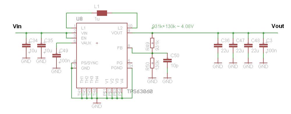
And, I'm pretty sure that the PCB layout is correctly designed. L1 is soldered about 2 mm from converter pads. Capacitors and resistors are also as close as possible. Power ground node is connected only in one point (under the device) with control ground node - very similar to the one shown in slvu442 (TPS63060 EVM).


Test discription:
There is applied steady load of 0.08 A to the output of the converter and everything is ok. When I increase load, the output voltage falls down and doesn't goes up while the load is applied. When I decrease the load, the Vout goes back to the ~4.1 V. The results are listed below (values are rounded):

Vin = 5.0 V

Iout = 0.08 A --> Vout = 4.1 V
Iout = 0.20 A --> Vout = 4.1 V
Iout = 0.40 A --> Vout = 3.9 V
Iout = 0.80 A --> Vout = 3.6 V
Iout = 1.20 A --> Vout = 3.3 V

I noticed that when I increase Vin to 6 V, the converter works better. The load value that causes Vout drop of ~3.9 V is about 0.80 A. The converter doesn't cope with load of 1.2 A (Vout = 3.6 V) in this case.


From my results I can claim that TPS63060 doesn't maitain output voltage on the designed level during the load addition.

Can someone help me with this problem, please?

  • It doesn't look like your load should be beyond what the converter can supply, so you need to check a few things.  First, measure Vin and Vout right across the input and output caps.  Voltage drops across wire and PCB trace can change the voltage you think you have.

    Then, you can check your thermal layout and see how hot the IC gets when it has the higher loads.  At higher temperatures, the amount of current it can provide decreases.

    Besides that, you can order the EVM and test it.  Your results will match the D/S curves (figures 1 and 2).

  • Ok. Firstly there is small voltage drop (about 100 mV) across wire, DC connector and PCB trace, tested at 0.90 A load. So, the actual voltage across the input caps is 4.9 V and corresponding Vout equels 3.19 V).

    I've been testing DC/DC component with mentioned load for about 20 minutes and it's only warm (about 40 ~ 50 degrees centigrade), I can easly put and hold my finger on it.

    Concluding:

    1) Load = 0.08 A, Vin = ~5.0 V (across input caps) --> Vout = 4.12 V (across output caps).

    2) Load = 0.40 A, Vin = 4.95 V (across input caps) --> Vout = 3.92 V (across output caps).

    3) Load = 0.90 A, Vin = 4.9 V (across input caps) --> Vout = 3.19 V (across output caps), Device_temp = ~ 40 ~ 50 degrees centigrade.

    What can cause this behavior in my application? Besides, in D/S there are fig. 1 and 2 like this: Output current vs input voltage. Why did you refer to this?

  • Figures 1 and 2 show the amount of output current you can achieve at a given input voltage.  These prove that the part can provide your output power at your input voltage.

    So, we need to figure out what is different between your application and the D/S circuit.  Your local FAE would be the one to contact to help you this in detail.  Or you could order the EVM and see the part do what it is supposed to--regulate the output voltage.