This thread has been locked.

If you have a related question, please click the "Ask a related question" button in the top right corner. The newly created question will be automatically linked to this question.

What are the Symptoms of bq77910a?

Other Parts Discussed in Thread: BQ77910A

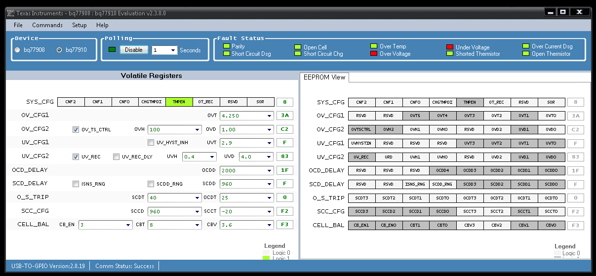
HI. I have a question.

What is a problem if the RED signal is turning on like on the Picture? I couldn't charge the pack anymore.

I think bq77910a is on the fritz. Is that right? How to avoid this problem?

Thanks

  • The part is seeing a simultaneous under voltage and over voltage.  There may be some contamination on the board causing 2 cell input pins (VCx) to pull together causing one cell to see a low voltage and one or both adjacent cells to see a high voltage.  Resistance to ground on a pin can also cause a high & low cell input voltage.

    If the part has been damaged by application of a voltage above abs max to the inputs, either on the single ended or differential limits, the pins could develop a resistive short to each other or to VSS internal to the IC.  This can also cause the simultaneous UV and OV.  Sometimes only 1 shows up depending on the applied voltage and severity of the damage.

    With the EVM a risk is removing the cell simulator with power applied to the board.  When one contact breaks at the end of the resistor divider, the inputs are pulled to the supply voltage by the remaining connection.  When wiring a board with separate cell connections, touching the cell tap to the wrong input can impose a high voltage on an input.  A tool or fixture path to ground could impose an unexpectedly high voltage on a cell input and potentially cause damage.  If connection is made with a connector and the wrong pins can contact during connector alignment, damage could occur with some combinations.

    While no input should exceed abs max, the VC1 and VC7 have shown to have some sensitivity to transients and were protected on the EVM.  Some users have indicated VC10 is also easily damaged and some protection on this pin may be needed.  Consider the system operating environment and what protections are needed and if it is on the product board or in the assembly fixture.

  • Thanks for Reply.

    I know that the Way of cell connection with BMS is in order of BATT-, CELL0, CELL1 ..... CELL10, PACK+,  is it right?

    Does it can cause damage to bq77910a If way of connection is wrong?

    I often connect a different order with cells.


  • Yes, bottom up connection is generally considered best.  Battery- connects to Vss of the IC and voltages are referenced to this point.  As cells are connected from the bottom up the differential capacitor pushes the upper pins up and as the BAT pin or other pack voltage capacitances charge, internal diodes push the upper cell inputs and the BAT voltage up.  The diode drop may be measured as a voltage which exceeds the abs max, but is current limited by the input resistances.  In some cases and where the current is not limited this may cause a problem and an alternate method must be used.

    The bq77910A was designed to anticipate random cell connection.  In general this works well.  Various tests at TI were successful but there are so many combinations of sequences that not all were covered.

    Connecting battery- first avoids negative voltages on input pins, which is generally bad for a device.  After this, a connection in the middle of the stack allows the lower differential capacitors to charge dividing the voltage between them.  The upper cell inputs bias as in the bottom up sequence.  When higher cells are connected, those charge the appropriate input capacitors and push up upper inputs.  When lower cells are connected, the inputs are already at approximately the same voltage and a small equalizing current flows in the input resistor.

    If the input is made with a connector which allows misalignment and a high voltage cell can make contact with a lower cell input, the input may exceed its abs max and be damaged.  An example of this might be on the EVM where the top cell group terminal block could be plugged into the lower cell input group board header.  Most likely the part would be damaged.

     Another possibility may be if the cell connections are made and broken.  If this occurs sequentially from the bottom, each time a higher connection is made, the voltage difference causes a current to charge all the capacitors in series.  The bottom capacitor will accumulate more charge and have a higher voltage than the upper capacitors. If a cell voltage exceeds its maximum, differential or single ended, damage to the device could occur.  Some users have indicated damaging the bottom cell during connection, this may be a possible cause.

  • Hi Thank you for Reply.

    I checked some faulty BMS applied BQ77910A. Most of BQ77910A were damaged at VC10.

    I think some PROTECTION on this pin  may be needed, Please advise on how to protect damage.

    thanks.

  • It would be best to determine the cause of the damage to know if the fix is effective.  If it is a cell transient during operation better filtering may help, if it is during connection, a fixture voltage limiting system may work and avoid cost in the product.

    In the bottom up connection sequence mentioned above, connections are assumed to make and stay connected.  When battery- is connected and remains, but the others connect and break sequentially bottom up, the VC10 voltage builds up.  Assuming a 4V/cell voltage, 4V, then 6V, then 7.33V...

    A zener/TVS on the lowest cell input will likely prevent the damage. You must pick a compromise between leakage and protection.  You would like zero leakage at normal cell voltage and clamp below the device VC10 ABS MAX limit of 5V, but ideal diodes don't exist so you must select a compromise. A zener clamp at VC10 would be more certain, but since abs max is 5V and the pin must swing to an induced voltage above this in normal balancing operation, the designers/datasheet author have given us a negative margin for selecting a zener.   If balancing is not used, a zener may be (more easily) placed on VC10.

    The zener on the cell input would clamp the cell transient if it is due to operation so that less comes through the filter.  It will also limit the voltage at VC10 during conneciton because once the diode conducts current will flow through the input resistor and diode to prevent excessive voltage build up on the capacitor.  VC10 can still see the voltage of the diode plus the voltage across the resistor.  If your zener diode limiter can be fixtured to the board during cell connection and removed after, it could be placed on VC10 for a more restrictive limit, then removed before operation.