This thread has been locked.

If you have a related question, please click the "Ask a related question" button in the top right corner. The newly created question will be automatically linked to this question.

TPS40305 is damaged when feedback resistance is dynamically adjusted

Other Parts Discussed in Thread: TPS40305, CSD17313Q2

Dear Sir/Madam,

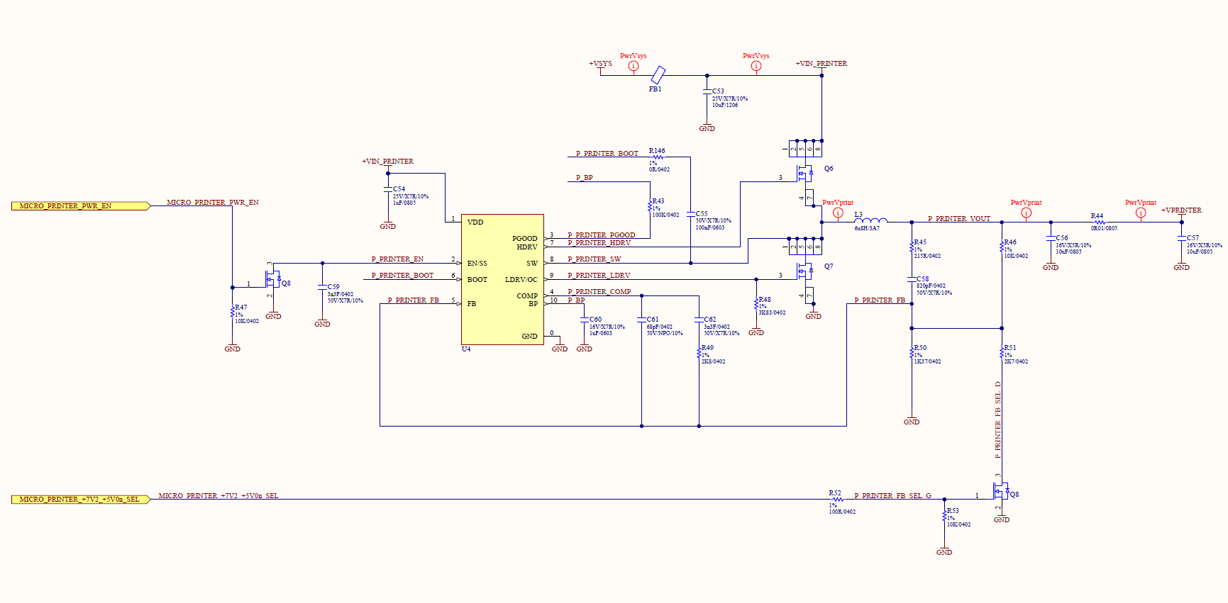
The circuit description that follows can be referenced to Figure 14 in "SLUS964A –NOVEMBER 2009–REVISED AUGUST 2012".

It is intended to dynamically change the feedback resistance (R5)  to alter the output voltage. This is accomplished using an NMOS FET and resistor in parallel with R5.

The NMOS gate is tied to GND using a 10K resistor to ensure +5V0 output is default unless driven high by micro.

It has been observed that if EN/SS pin is tri-stated (TPS40305 enabled) and the feedback resistance is changed the TPS40305 is damaged.

Appears that the parts does not start and the LDR/OC drive is damaged. You can see a periodic saw tooth waveform on C1 of less than 1V and the

FB voltage is less than 0.6.


Interestingly if you do the following the TPS40305 is not damaged and works perfectly.

(1) Pull EN/SS to GND (TPS40305 disabled)

(2) Make the feedback resistance change.

(3) tri-state EN/SS pin (TPS40305 enabled)


It will be difficult to ensure that software does violate this procedure.

My question is, how do i protect the TPS40305 to be able to dynamically adjust the feedback resistance without damage.

Regards Grant

  • Hi Grant,

    What is the value of R4, R5 and the resistor in parallel with R5 you used for dynamic Vout change? Is the NMOS in series with the resistor, right? The part got damaged when the NMOS turns on or off?

    How do you know the LDR/OC drive is damaged? My understanding is if only LDR/OC drive is damaged, the converter will still work. The synchronous FET (Q1) will work as diode without LDR drive. Extra loss and less efficiency but the circuit should still work.

    Are there any damage to the power mosfets (Q1, Q2)? If the voltage on C1 is saw tooth, the part is likely in the overcurrent protection mode. If there is no damage to the power mosfets, it is likely not a real overcurrent condition and might be caused by high-side driver damage.

    Is there any way the software could slow down the turn on/off speed of the NMOS? You may consider parallel a cap to the 10kohm resistor between NMOS gate and GND. I suspect the fast transient may cause problem but I still think your approach for dynamic Vout change should work.

    Regards,

    Na

  • Hi Na,

    Please see schematic below. R4 =R46 = 10K. R5=R50=1K37 NMOS FET off. 1K37 in parallel with 2K7.

    LDR/OC was just an assumption.

    Q1 and Q2 are not damaged because we replaced the TPS40305 and is worked again with NMOS FET OFF(switching disabled).

    It is possible to slow the NMOS FET turn on but we are running out of parts to keep trying different options.

    Regards Grant

  • Hi Na,

    Q6 and Q7 are CSD17313Q2. If we can take this offline then i have some scope shots and more information that i can share. It would be nice to understand why the TPS40305 is being damaged

    before i start the experimenting with Q8 turn on/off.

    Regards Grant

  • Hi Grant,

    You may send me you email address and I will contact you offline.

    What is the input voltage? You may check whether you can measure the BP to BOOT diode on the broken IC. I suspect during transient, the BOOT voltage may experience overvoltage to cause damage to BOOT diode.

    Regards,

    Na

  • Hi Na,

    The input voltage is 12V. I will take some measurements.

    Regards Grant