This thread has been locked.

If you have a related question, please click the "Ask a related question" button in the top right corner. The newly created question will be automatically linked to this question.

LM3100MH Input pins explode

Other Parts Discussed in Thread: LM3100, LM5574

I have been using the LM3100MH to convert 26V to 6.5V at 250mA in a textbook application for several years. Recently I am seeing a large number of regulators that have pins 4 and 5 (Vin) blown off the board when power is applied to the circuit. I do not think there is a chance I have significant load current, so am thinking there might be a possibility that the input voltage is spiking above the 40V limit or possibly negative. Any thoughts as to the most likely cause of this catastrophic failure and the best way to fix it? My input voltage can be between 17V and 30V. When failure occurs the regulator is the only component damaged.

  • Hello David, 

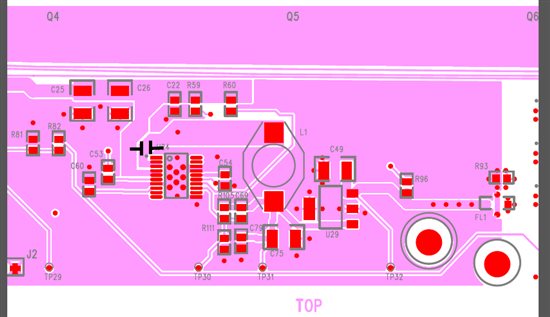
    Would it be possible to share your board layout and schematic?

    Non ideal placement of the input cap in buck converters can cause large switching spikes. See this post for example. 

    http://e2e.ti.com/support/power_management/simple_switcher/f/858/t/222780.aspx

    Regards, 
    Denislav 

  • Hi David,


    1 comment and a couple questions.

    Comment:  I looked at your layout and I think that you would see less noise on your design if you moved one of your ceramic capacitors like the blakc drawn in one here.  This will help to reduce high frequency noise on your ground plane and should help lower the noise on all of your signals.

    That being said, I am not sure that that is what is causing your failures.


    Questions:

    Where is the input voltage of the LM3100 coming from?

    Is the slew rate of this voltage controlled on start-up?

    Do you have a higher esr capacitor, such as an electrolytic somewhere in the design to damp overshoot or oscillations from a hot plug or fast turn on transient?


    Regards,

    Marc


  • Thanks Marc.

    The input voltage normally comes from either a 25V battery array (lithium or lead-acid) or an external battery charger (25-29V). There is no slew rate control on the source and no additional capacitance on the input.

    The place I am seeing the failures is when I connect this to our production test equipment, which includes a programmable power supply. The supply seems to have a well-controlled ramp at power-up(5-10ms), but there may be cases I am not seeing where the slew rate is greater.

  • OK,

    Possibility1:

    If the leads that you are connecting the to the programmable power supply are long then they can have significant inductance.

    The Inductance plus the ceramic input capacitors plus the negative impedance of a buck regulator can create a very good oscillator.

    I would check the input voltage at a lower value like 16Vin (so as not to damage the part) and see how much variation you have in Vin.  If this is the problem, the solution is to add an electrolytic or other high esr capacitor to damp the Q in the LC resonant tank.  There is an equation and spreadsheet for this in AN-2162 Simple Success with conducted EMI.  But that requires you to know the inductance.  For a first pass try a 50V 100uF electrolytic capacitor with ~100mohms of ESR and place it close to your ceramic input capacitors.

    Possibility 2:

    The extra noise from your capacitor placement is causing the input voltage spikes to pass the abs max of the part.  Try adding a 1uF leaded capacitor to your design in the location mentioned in my previous post.  Cut the leads to be as short as possible and still span the switch node.


    Try those two things out and let me know if you see some improvement.


    Regards,

    Marc


  • I will try these additions.

    As part of a CCA re-spin I am thinking of changing to a higher voltage regulator (LM5574) to provide more of a safety margin in case someone hooks this up to a higher supply voltage. Would you recommend this part?

  • The LM5574 is a good part.  If you redesign using that part, just remember that the INput capacitor, LM5574 and catch diode is the primary current loop and needs to be as small as possible, with the capacitor as close as possible to the input of the 5574 and the anode of the catch diode.

    One other thing, you mentioned possible negative voltages in your original post.  If this is still a concern you can connect a diode in series with the input voltage to protect the part.


  • David,

    To add to what Marc mentioned about LM5574, you can take a look at the WIKI page for example placement of the power stage components along with some guidelines. Here is a link:

    http://e2e.ti.com/support/power_management/simple_switcher/w/simple_switcher_wiki/2215.lm5574lm25574-pcb-layout.aspx

    Regards, 
    Denislav