This thread has been locked.

If you have a related question, please click the "Ask a related question" button in the top right corner. The newly created question will be automatically linked to this question.

LP38501-ADJ Linear Drop-out Reagulator Vout calculation

Other Parts Discussed in Thread: LP38501-ADJ

I'm using LP38501-ADJ to supply my GSM modem.. It's output is adjustable from 0.6V to 5V. I'm supplying it with 5.1V input. The formula given for calculation of output voltage is  

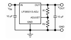
I kept R2=10K ohm, V  adj = 0.605v, I adj=750nA, required Vout = 4V so i got R1 = 56K ohm.. Is this correct?

But when i connected as per the above mentioned resistors, i'm getting no change in Vout. It's same as input Vin=5.1v. and V adj = 3.5V. It's not 0.605V.

1) What should i substitute for V adj and I adj?

2) What value of resistors (R1 and R2) should i use to get Vout = 4v?

Please help... 

  •  

    Q: "... What value of resistors (R1 and R2) should I use to get Vout = 4v? ..."

    With R1= 56k, R2= 10k, Vadj= 0.605V (typical) with Iadj= 50nA (typical), the Vout should be at 3.976V (typical)

    With +/-1% tolerances your output voltage should be in the range of 3.870V to 4.085V.

     " ... Vout. (is) same as input Vin=5.1v. and V adj = 3.5V. It's not 0.605V..."

    Something is not right.

    Is your measurement of Vadj=3.5V at the ADJ pin (device pin 5), or at the connection between R1 and R2?

    With Vout at 5.1V, R1=56k, R2=10k, and the connection the ADJ pin open, the voltage across R2 should be closer to 0.773V.


  • "..Is your measurement of Vadj=3.5V at the ADJ pin (device pin 5), or at the connection between R1 and R2?"

    Vadj=3.5V between the ADJ pin (device pin 5) and Ground pin (device pin 3) .. 

    I have used 100uF capacitor at input side and 330uf capacitor at output side..but in the diagram 10uF capacitor is used. Is that OK?


  • The resistors was not connected properly with top layer of PCB and now i'm getting Vout=3.9V..