This thread has been locked.

If you have a related question, please click the "Ask a related question" button in the top right corner. The newly created question will be automatically linked to this question.

Discrepancy between bq77910A datasheet and bq77910AEVM schematic

Other Parts Discussed in Thread: BQ77910A

I found a discrepancy between the bq77910a part data sheet and the bq77910AEVM evaluation module schematic for the CPCKN and CCAP pins.  

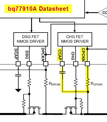
The bq77910A data sheet (SLUSAV6-FEBRUARY 2012) on page 33 shows a series connection of a capacitor and a resistor between the CPCKN and CCAP pins.


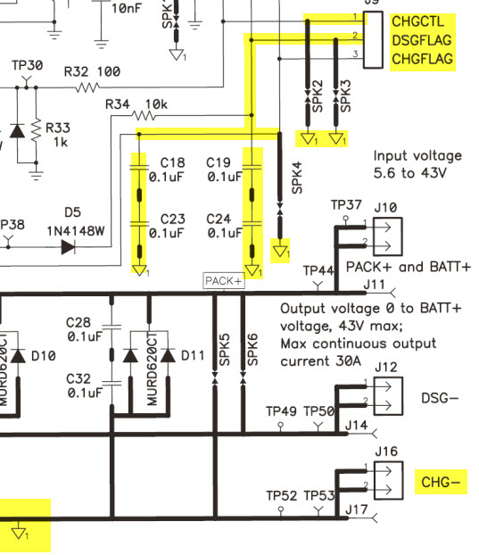
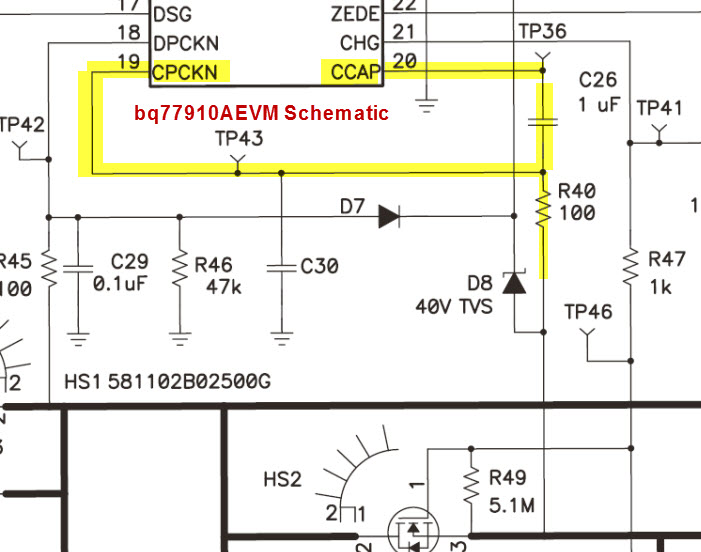
The bq77910AEVM User's Guide (SLUU855-February 2012) on page 30 shows a capacitor connected between CPCKN and CCAP with no series resistor.

Which connection is correct and why?

Also, referring to the bq77910AEVM schematic on page 30, what is the purpose to C18, C19, C23 and C24.  Why are they both tied to CHG- return.  Would it be better to connect the DSGFLAG bypass capacitors to DSG- instead of to CHG-?  The spark gaps are also all connected to CHG- ground.  What is the the reason for the ground selection.

  • I have updated my original post with images showing the discrepancy between the bq77910A datasheet and the Evaluation module schematic.  This should make it easier to see the discrepancy between the two.

    Does anyone have an idea as to which of these two configurations is the correct one?

    Thanks.

  • Regarding the CCAP capacitor placement: The device regulates CCAP with respect to CPCKN, so the capacitor connected at the CPCKN terminal is best for the regulator.  It also avoids transients pushing up CCAP.  This connection will have some effect when the part turns on the CHG output and the capacitor charges the gate of the FET.  See www.ti.com/lit/slua612 sections 6 & 7.  Either position can work, the EVM placement should be safer for the IC.

    The capacitors C18, C19, C23 and C24 are to provide ESD protection for the flag outputs.  The expectation with the EVM is that the user could short the power FETs and use the flag outputs as the board outputs.  The diodes were provided in the flag ouptuts so a user could not back drive the device outputs by trying to use both the flag outputs and FETs.  With the FETs shorted or without, CHG- is potentially the most negative voltage in the system. Since the DSG- also connects back to the sense resistor, it could have been used, but if the board was converted to series FETs, CHG- would be the output terminal.  So the CHG- terminal was used.

    Note that a highly configurable EVM like this one does not represent a finished product and the ESD design may need further development for use in a product.

  • Thank you for the response. 

    I reviewed the documents you suggested and see that the series FET configuration requires some thought and analysis.  In my application, I am using a parallel FET configuration.   Can I assume that the short circuit transients, addressed in the series FET case, do not apply to my parallel FET design?

    Thanks

  • Correct.  CPCKN range should be limited by the FET arrangement and should not be able to reverse voltage with BAT and push up the BAT pin.  You will still need to watch the effect of the SC response on the device inputs through the filters and clamps.  DPCKN will need its filter to keep transients in a safe range.  Always test thoroughly.

  • Thank you for your suggestions to test thoroughly.

    I am planning to incorporate several test points on my custom design and would appreciate your ideas on where to place them for a parallel FET configuration.  The article you referred to described the key device inputs to monitor for a series FET configuration.  What are the key device inputs I should monitor for the parallel FET configuration?

  • Basically all the same inputs.

    Most signals are referenced to VSS, so you want that easy to access. When your load is switched off you may want to check transients from the cell filter to input pins and to BAT.  When the device protects against discharge you may want to see DPCKN.  On charge cutoff you may want to see BAT - CPCKN.  You could observe sysetm currents, or you may want to see CHG and DSG.  For checking behaviors you may want to see CHGST, VREG and TS

    You will likely have test points on your production board, but during development you may want them more prominent.