This thread has been locked.

If you have a related question, please click the "Ask a related question" button in the top right corner. The newly created question will be automatically linked to this question.

TPS54060 in inverting application: possible layout problem

Other Parts Discussed in Thread: TPS54060

Hi,

our customer copied the split rail EVM, but on their prototype they have measured the waveform on L1 pin 1, different from the EVM. The waform is attached:

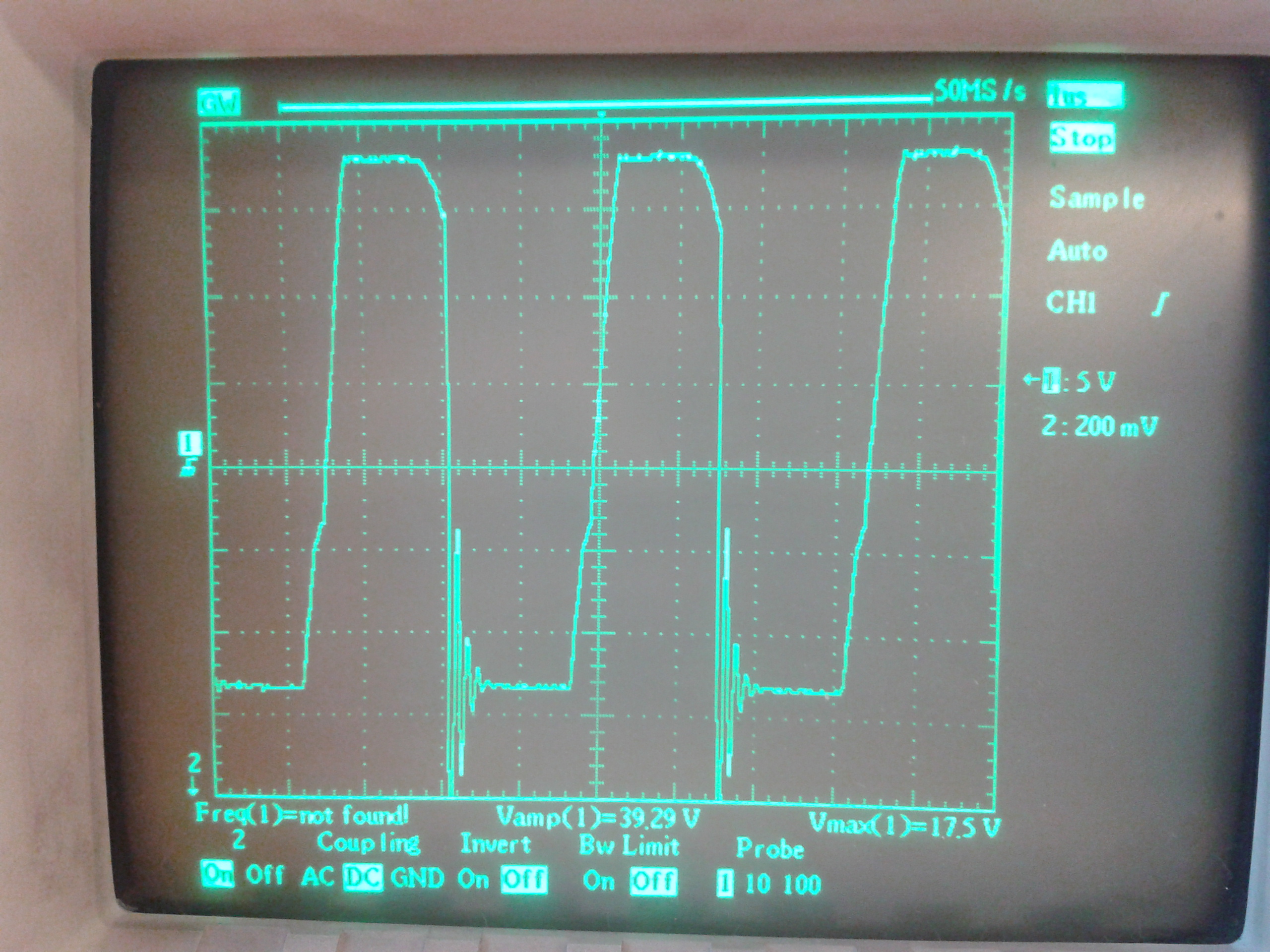
This type of a waveform then spoils the input of the LDOs that can't filter out the noise. It looks to be a layout problem, can you advise the possible reason and the points we need to check in this case. 

  • Hi Dmitry,

    I have a few questions to get familiar with this issue.

    Is the ringing when the switch turns off what they believe to be the source of the noise? Also what is the load current for this measurement? Lastly, were there any changes made to the customer's layout and schematic for the TPS54060 when compared to the EVM?

    Best Regards,
    Anthony

  • Anthony,

    the load current is expected at 100 mA, the load is the LDOs TPS7A for cleaning the ripple. The main difference from EVM is the shrink of the layout to the dimension 18x21 mm. The question is it possible to optimize the PCB to this tight dimension? There were no changes in the circuit at all.

    we suppose the main source of the overshoot is the presence of parasitic capacitances. Most probably there is parasitic coupling due to a tight PCB dimension.

    What you think if we increase the switching frequency to shrink the dimensions of the components? Can this help to minimize the influence of the smaller poligons in the Prototype PCB?

  • Dmitry,

    I think the layout will be able to be optimized even to the smaller size. Can you share they layout they are testing? I would guess some things had to be shifted to fit within this area. It's important to keep all current loops as small as possible. The key one in the inverting buck boost is through the input capacitor, the TPS54060, and the windings of the inductor.

    If it is the ringing during turn on or turn off of the FET or one of the diodes, adding a snubber to the two switching nodes should help.

    Best Regards,
    Anthony

  • Hi, can you send me your e-mail connect, posting PCB layout to forum could be sensitive.