


Hi,
This is Arumugam from India.Im using the TPS54331 Buck converter in my design and my layout portion is attached below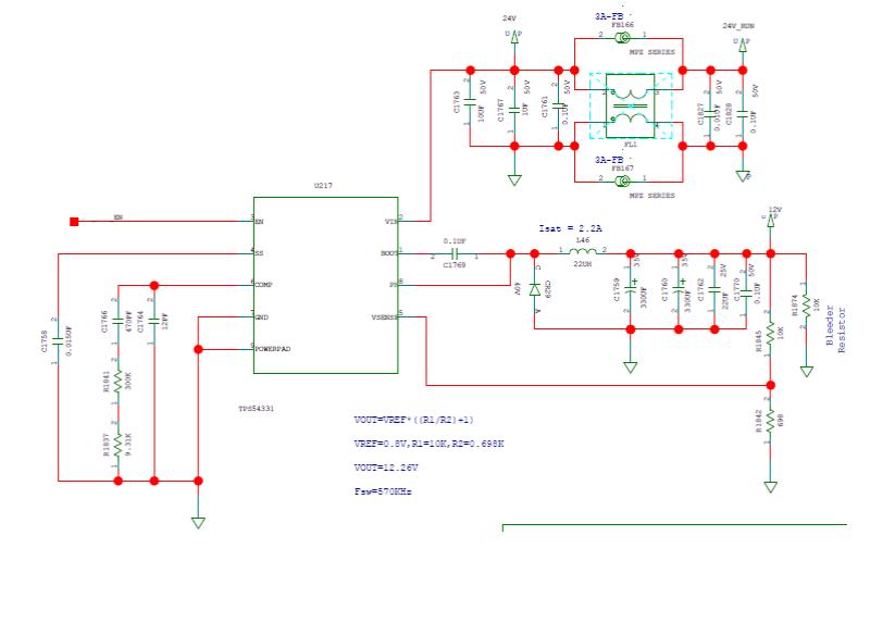
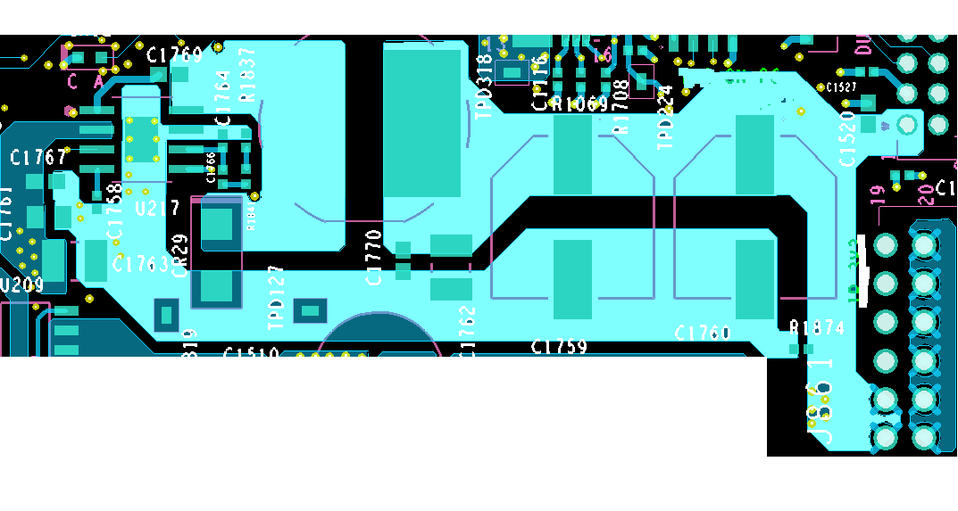
In the layout ,the input common mode choke and ferrite bead is placed at the bottom side exactly at the inductor place.To avoid the Gnd loop ,the output gnd and capacitor gnd is connected to the TPS54331 thermal pad and at thermal pad only we were provided 10vias toGND.And no vias we added at the output bulk capacitor section.This practice we did for avoid the gnd loop,since the board layer 2 is Gnd,so if we add stitching vias then we might have many return path for the 12V gnd.
Whether our method of grounding is ok or need to provide the stitiching vias at the output capacitor also.
Pls share your thoughts .
Thanks-Arumugam
