This thread has been locked.

If you have a related question, please click the "Ask a related question" button in the top right corner. The newly created question will be automatically linked to this question.

TPS65381-Q1 Component Values - Reverse Polarity

Expert 1485 points
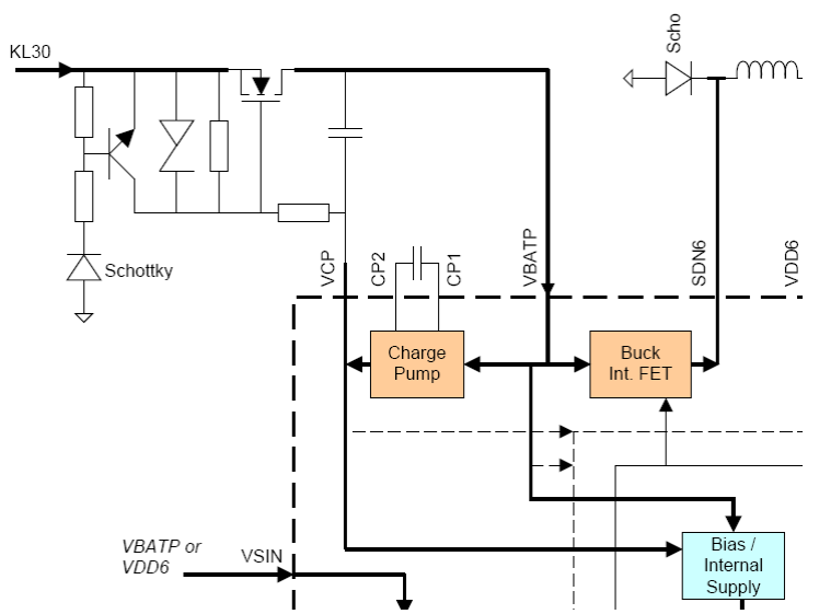
Other Parts Discussed in Thread: TPS65381-Q1

Does TI have a recommendation for component values for the TPS65381-Q1 reverse polarity circuitry as shown in the figure below (specifically resistor / capacitor):

  • Rustin,

    Do you have the latest Data Sheet? Fig 21 on pg. 57 shows the part values. See http://www.ti.com/lit/ds/slvsbc4/slvsbc4.pdf

  • Thanks for the updated datsheet.  I see the capacitor is shown as 100nF (50V).  What about the remaining comonents…are these needed?  Is there any specific requirements on the resistor values for RG, RGS, and the values surrounding the NPN?

  • Hi Rustin,

    After more research, the data sheet text indicates that the Vcp to FET gate resistor s/b 10k ohms to keep Vcp within the Abs Max voltage range when the battery is reversed. The resistor divider from Vbat In to Vcp is needed to generate the proper gate voltage to keep the FET on when the battery is in normally. The bipolar NPN is off when the battery is in correctly but on (as a switch) when the battery is reversed to keep the FET off. I believe that the zener in the circuit is there to protect the FET. Short of designing this from scratch, I haven't been able to locate any design info on this circuit except for here .....Note: Link Deleted

  • Jeffery,  the link above takes me to a page that says "Group not found".  Do you have a new link?

  • Rustin,

    I'll send you an e-mail.

  • All,

    The schematic in the datasheet showing the reverse protection just as suggestion to give the customer a hint how to protect the device against reverse polarity. It’s customer responsibility to define the circuit details under working conditions. To give you an idea how it works, I will show you an example:

    To reduce the voltage drop across the NMOS transistor  in normal operation, the charge pump voltage VCP is used to turn it on. The VCP voltage above battery is between +4 and +15V, please see parameter 8.1 in  datasheet. To keep the load to the charge pump to the minimum, the resistors should have relatively high. The resistor can be calculated by VGS=VCP divided by the max allowed current.

    In real automotive applications external resistor should be usually not above 100kOhm(leakage during high humidity). If we assume the 100kOhm resistor and  a max. VCP=VGS=15V, the circuit will take 15V/100kOhm=150uA out of the charge pump. The Gate-Source zener diode should have a breakdown above the max. VCP to avoid any extra current but protect the Gate Source of the NMOS transistor.   

    To limit the current out of VCP in reverse conditions, the resistor between VCP and the gate should be in the range of a few kOhm. If the resistance is too high it would build a resistor divider for normal operation together with the G_S resistor and that would limit the GS voltage causing a higher RDSon of the NMOS transistor and so a higher voltage drop for a given current.

    For reverse conditions the NPN should discharge the gate of the NMOS transistor. To do that a VBE of about 0.7V is needed to turn on the NPN. The resistor from the base of the NPN to the schottky diode is mostly defining the current during reverse conditions e.g. at -14V. Both resistors are building a voltage divider and defining together with the VBE of the NPN and the schottky voltage the negative ON voltage of the protection circuit.

    If you have any further questions, please let me know.

    Thanks and regards

    Michael